Intel’s Tunnel Falls: 24,000 Quantum Chips Per Wafer and the Manufacturing Argument Made Real
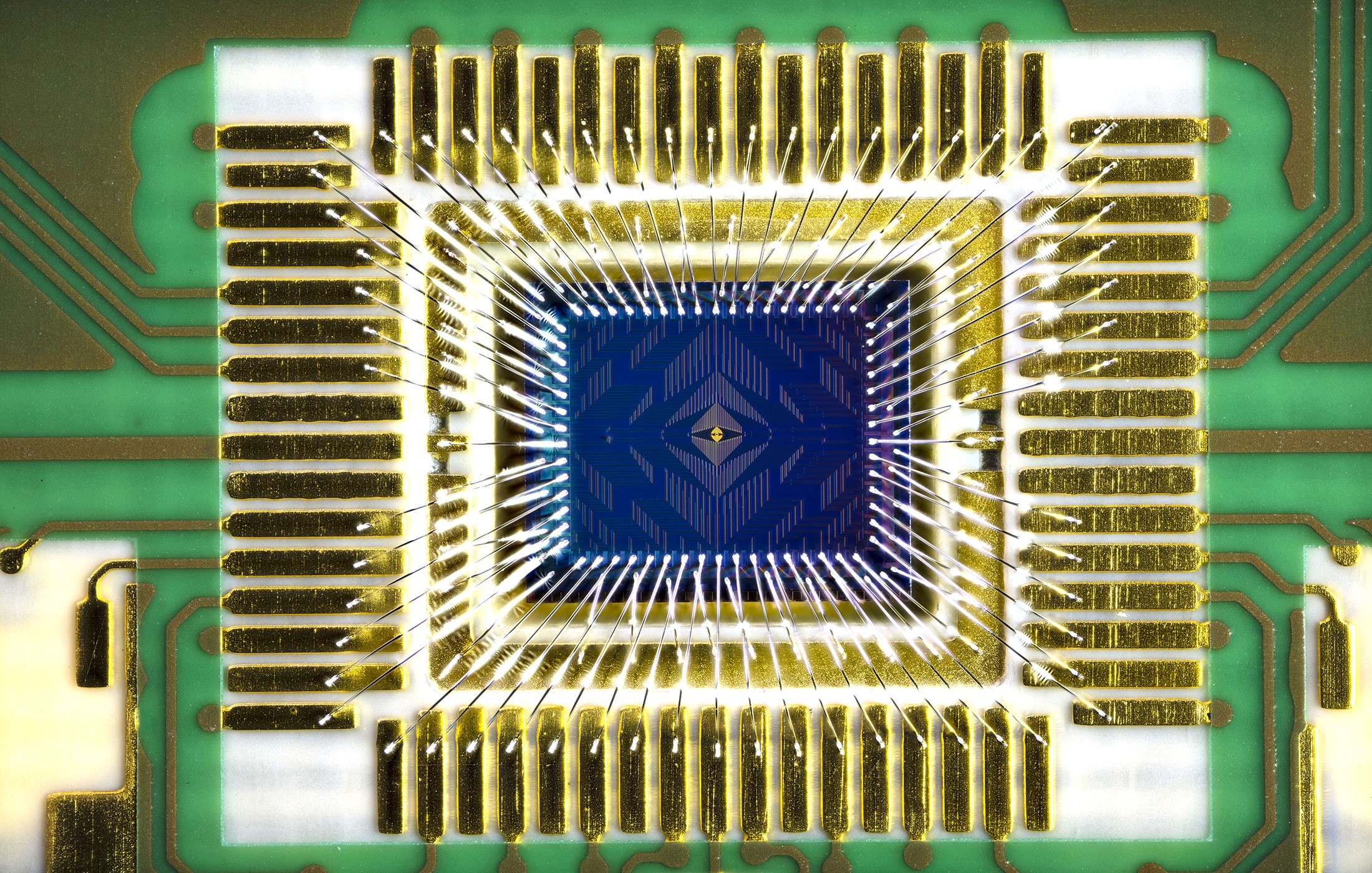
Table of Contents
22 Jun 2023 – Every conversation about silicon spin qubits eventually arrives at the same claim: because these qubits are essentially single-electron transistors, they can be manufactured using the same processes that produce billions of classical transistors every year. The implication is staggering — a scalable quantum computer rolled off a semiconductor production line, not hand-assembled in a physics lab.
It has always been a compelling argument. It has also, until now, been largely theoretical. The silicon qubit groups delivering the best performance — SQC in Sydney with its atomically precise donor qubits, academic labs in Delft and Tokyo — use bespoke fabrication techniques: scanning tunnelling microscopes, electron-beam lithography, one-off devices. These produce world-class qubits, but they do not prove the manufacturing thesis.
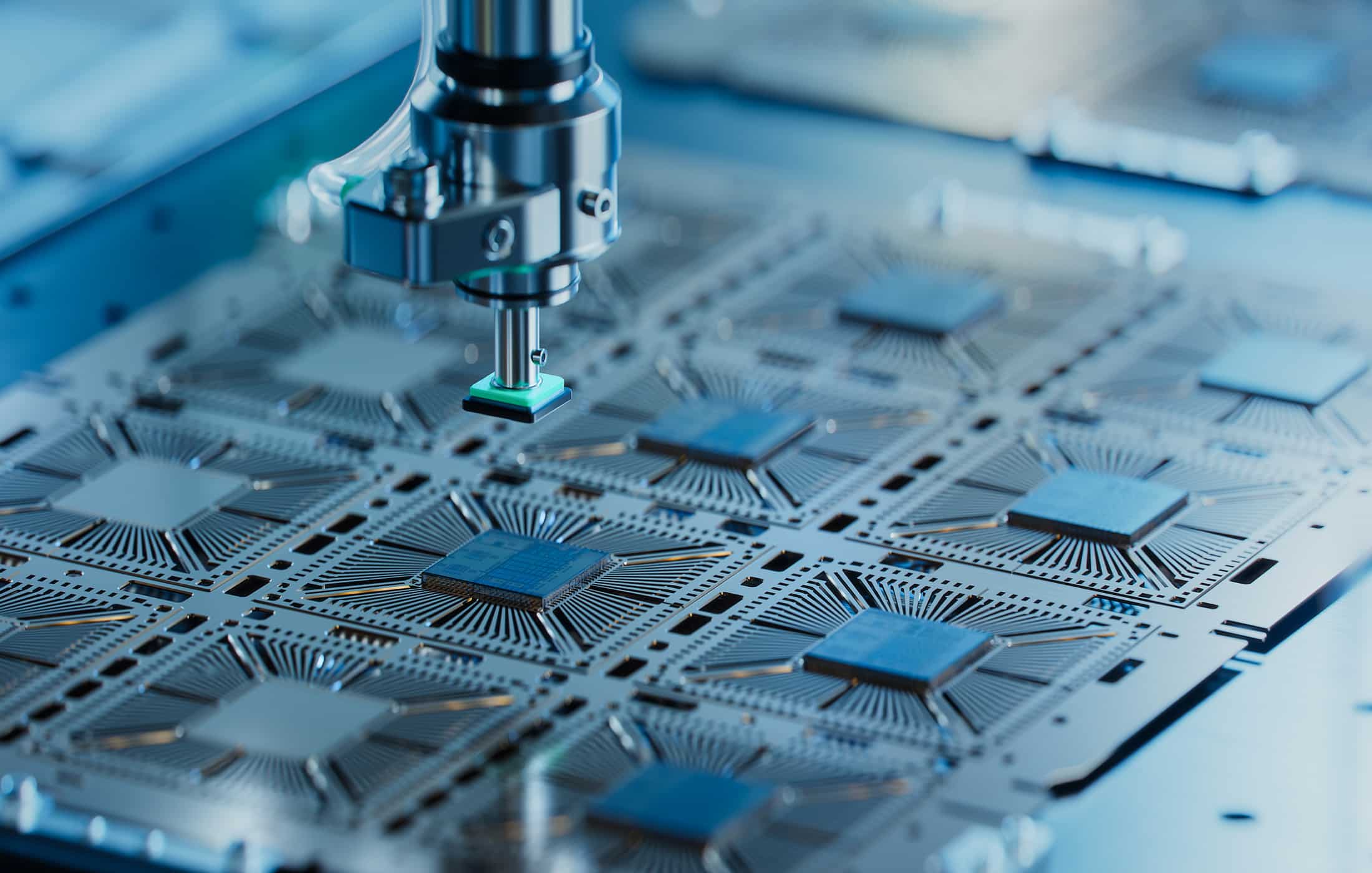
Intel just did. The company has released Tunnel Falls, a 12-qubit silicon spin qubit chip fabricated on 300 mm wafers at Intel’s D1 research facility in Hillsboro, Oregon, using the same extreme ultraviolet (EUV) lithography and gate processing techniques that produce Intel’s commercial processors. Published in a companion technical paper and announced through a partnership with the Laboratory for Physical Sciences at the University of Maryland, Tunnel Falls is the first silicon spin qubit device made available to the broader research community — and the first to demonstrate that quantum dot qubit fabrication can achieve the yield and uniformity that industrial semiconductor manufacturing demands.
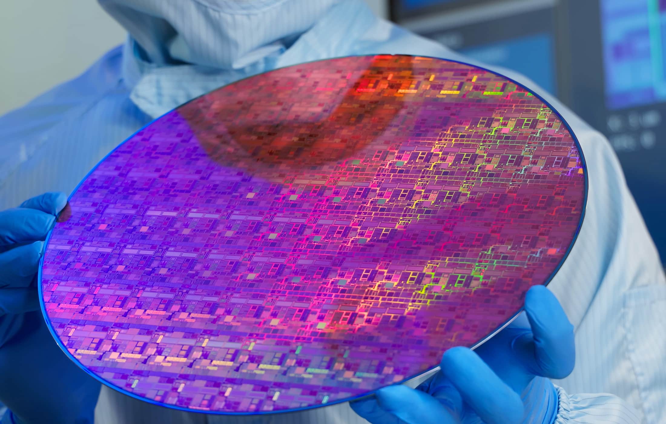
The headline numbers: 95% yield across the wafer. Over 24,000 quantum dot devices per wafer. Voltage uniformity comparable to standard CMOS logic processes.
These are not qubit fidelity records. They are manufacturing records. And for the long-term trajectory of quantum computing, they may matter more.
What Tunnel Falls Is — and Isn’t
Tunnel Falls is a linear array of 12 quantum-dot spin qubits fabricated in a Si/SiGe heterostructure. Each qubit is a single electron trapped under a transistor gate, with the electron’s spin state (up or down) encoding the quantum information. The gate layout — screening gates, plunger gates, barrier gates — is designed to be compatible with standard semiconductor fabrication rules, avoiding the bespoke overlay structures and lift-off processes that most academic silicon qubit devices still require.
The chip is fabricated using Intel’s standard 300 mm wafer processing line, with immersion and EUV lithography defining gate features at pitches ranging from 45 to 100 nm. This is not a process developed specifically for quantum computing — it is Intel’s existing transistor fabrication capability, adapted with relatively minor modifications for qubit devices.
What Tunnel Falls is not: a high-performance quantum processor. Intel has been measured about qubit fidelity claims for this device, and the emphasis has been on fabrication metrics — yield, uniformity, reproducibility — rather than operational benchmarks like gate fidelity or coherence time. Jim Clarke, Intel’s director of quantum hardware, has been explicit about this: “For us, it’s less about the number [of qubits] and more about the quality.” The quality Intel is optimizing first is fabrication quality, not gate quality.
This is a deliberate strategic choice. Intel’s thesis is that solving the manufacturing problem first — proving that qubits can be produced at industrial scale with industrial uniformity — creates the foundation on which performance optimization can then proceed. The alternative approach, pursued by groups like SQC, is to optimize performance first using bespoke fabrication, then figure out how to manufacture it. Both strategies are legitimate. They are bets on which bottleneck will prove harder to solve.
Why Manufacturing Metrics Matter
For a community accustomed to tracking gate fidelities, coherence times, and qubit counts, Tunnel Falls’ emphasis on yield and uniformity may seem underwhelming. It shouldn’t be.
Consider the arithmetic. A fault-tolerant quantum computer will need millions of physical qubits. Fabricating these qubits one at a time with an STM is not a viable path to that scale — not because the physics doesn’t work, but because the economics don’t. You need a manufacturing process that produces qubits in bulk, with predictable performance, at a cost that scales sublinearly with qubit count.
That is exactly what a semiconductor fabrication line does. And Tunnel Falls demonstrates that silicon spin qubits are compatible with one. The 95% yield means that of the roughly 25,000 devices on a single wafer, approximately 24,000 are functional. The voltage uniformity means that these 24,000 devices behave similarly enough that control parameters calibrated for one device are likely to work for its neighbours — a prerequisite for the automated calibration routines that any large-scale quantum processor will require.
The practical implication: if Intel (or any other semiconductor manufacturer) can solve the remaining performance challenges — getting gate fidelities above the fault-tolerance threshold in foundry-fabricated devices — the path from “working qubits” to “millions of working qubits” is paved by existing manufacturing infrastructure, not by inventing new fabrication paradigms.
The Democratization Strategy
Beyond the chip itself, Intel’s decision to distribute Tunnel Falls to research labs is strategically significant. Through the Qubits for Computing Foundry (QCF) programme — a collaboration with the U.S. Army Research Office and the LPS Qubit Collaboratory — Intel is placing Tunnel Falls chips in the hands of researchers at Sandia National Laboratories, the University of Rochester, the University of Wisconsin-Madison, and others.
This is unusual. Most quantum hardware companies guard their chips closely. Intel is doing the opposite — deliberately building an ecosystem of researchers who have hands-on experience with its qubit platform, who will develop control techniques, discover error modes, and publish results that feed back into Intel’s development cycle.
The strategy has a practical logic: Intel makes chips; it does not (primarily) do quantum physics research. By putting chips in the hands of physicists, it gets the physics exploration done in parallel with its own engineering optimization, at a fraction of the cost of building an in-house quantum physics lab of comparable breadth.
For the silicon qubit field generally, the move is constructive. One of the barriers to progress in semiconductor qubits has been that only a handful of labs worldwide have the fabrication capability to make them. If Intel can supply high-quality, reproducible devices to dozens of labs, the pace of discovery accelerates — not just for Intel’s platform, but for the understanding of silicon spin qubits generally.
Where This Sits in the Silicon Landscape
Tunnel Falls occupies a specific and important position in the broader silicon quantum computing ecosystem.
At one end of the spectrum are the atomically precise donor qubits from SQC — phosphorus atoms placed individually using STM lithography, achieving the highest gate fidelities in silicon but requiring fabrication techniques that do not yet scale to industrial volumes.
At the other end is Tunnel Falls — gate-defined quantum dots fabricated at industrial scale with industrial yield, but with performance characteristics that haven’t yet been fully benchmarked against the fault-tolerance threshold.
In between sits a growing middle ground: groups like Diraq (working with GlobalFoundries on 22 nm CMOS integration) and Quantum Motion (pursuing silicon quantum error correction with cryo-CMOS integration) are attempting to combine foundry-compatible fabrication with high-fidelity qubit operation. The question for the field is whether these approaches can converge — whether foundry-manufactured qubits can reach the fidelity levels that bespoke devices have demonstrated.
Tunnel Falls does not answer that question. But it proves that the manufacturing side of the equation is solvable, which shifts the burden of proof squarely onto the performance side. And that, for a technology whose entire value proposition rests on manufacturing scalability, is a significant step.
Implications for Quantum Security
Tunnel Falls’ relevance is structural rather than immediate. No 12-qubit device threatens any cryptographic system. But the manufacturing proof-of-concept it represents has implications for how quickly silicon quantum computing could scale once the performance requirements are met.
The standard threat model for a cryptanalytically relevant quantum computer implicitly assumes that building millions of qubits will be hard regardless of platform. Tunnel Falls suggests that for silicon, the manufacturing part may not be the bottleneck — the bottleneck is qubit performance and error correction, not fabrication throughput. If and when silicon qubits achieve fault-tolerant operation, the manufacturing infrastructure to scale them already exists.
That “if” remains substantial. But the list of remaining obstacles just got one item shorter.
Quantum Upside & Quantum Risk - Handled
My company - Applied Quantum - helps governments, enterprises, and investors prepare for both the upside and the risk of quantum technologies. We deliver concise board and investor briefings; demystify quantum computing, sensing, and communications; craft national and corporate strategies to capture advantage; and turn plans into delivery. We help you mitigate the quantum risk by executing crypto‑inventory, crypto‑agility implementation, PQC migration, and broader defenses against the quantum threat. We run vendor due diligence, proof‑of‑value pilots, standards and policy alignment, workforce training, and procurement support, then oversee implementation across your organization. Contact me if you want help.
Related Content