Three Bets on Silicon: Donor Qubits, Quantum Dots, and the Foundry Path Compared

Table of Contents
When people say “silicon quantum computing,” they often speak as if it is one thing. It is not. It is at least three distinct approaches, built on the same material but employing different physics, different fabrication methods, and different strategies for reaching fault-tolerant scale. Understanding these differences — and the tradeoffs each makes — is essential for anyone tracking which version of silicon quantum computing is most likely to matter, and when.
All three approaches share silicon’s core advantages: compatibility with semiconductor industry infrastructure, small qubit footprint (~50 nm), and long coherence times enabled by isotopic purification of ²⁸Si. But they diverge sharply on how qubits are defined, controlled, and manufactured.
Approach 1: Atomically Precise Donor Qubits
The idea: Embed individual phosphorus atoms into a silicon crystal and use their nuclear spins (or the spin of the donor’s extra electron) as qubits. Multiple donors placed within a few nanometres of each other share a single electron, creating a tightly coupled register with native multi-qubit connectivity through the hyperfine interaction.
Who’s doing it: Silicon Quantum Computing (SQC) in Sydney (Michelle Simmons), the Shenzhen International Quantum Academy (SZIQA) in China, and Andrea Morello’s group at UNSW.
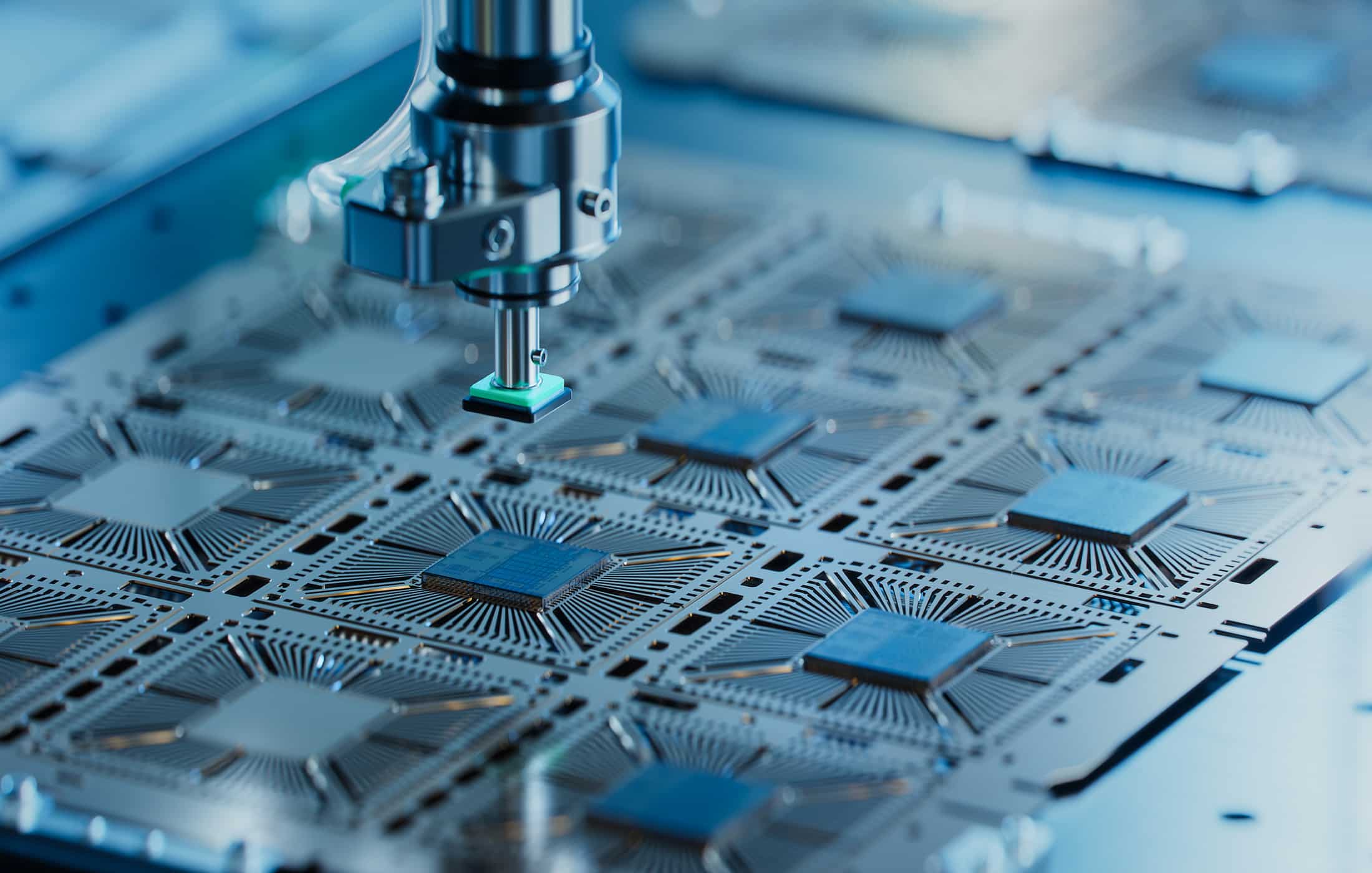
Fabrication: Scanning tunnelling microscopy (STM) hydrogen lithography. Individual phosphorus atoms are placed with sub-nanometre precision by selectively removing hydrogen atoms from a passivated silicon surface, then dosing with phosphine gas. This is atomic-scale fabrication — extraordinarily precise, but slow and not yet industrially scalable.
Strengths:
The donor approach delivers the best raw performance in silicon by a significant margin. SQC’s 11-qubit atom processor demonstrated two-qubit gate fidelities of 99.9% — a silicon record — with single-qubit fidelities up to 99.99%. Nuclear spin coherence times reach seconds, enabling deep circuits without decoherence bottlenecks. The hyperfine-mediated multi-qubit gates provide all-to-all connectivity within a register, reducing circuit depth compared to architectures requiring SWAP routing. SZIQA has demonstrated the first universal logical operations and stabilizer-based error detection in silicon, both using donor clusters.
Weaknesses:
The STM fabrication process is inherently serial — each donor is placed one at a time. Current devices take weeks to fabricate. Scaling to thousands or millions of qubits using STM lithography faces daunting throughput challenges. Inter-cluster connectivity (linking separate donor registers) has been demonstrated only once, in SQC’s 11-qubit device, via electron exchange coupling — and the 13 nm inter-register distance requires atomic-precision placement that becomes harder as arrays grow. Cross-talk between closely spaced donors within a cluster remains the dominant error source.
The bet: Solve the hardest physics problems first (fidelity, error correction, logical operations) using the cleanest possible qubits, then figure out how to manufacture them. The implicit assumption is that fabrication technology will eventually catch up to the physics.
Approach 2: Gate-Defined Quantum Dots
The idea: Use tiny transistor-like structures (quantum dots) to confine individual electrons in a silicon-germanium (Si/SiGe) or silicon metal-oxide-semiconductor (SiMOS) heterostructure. The electron’s spin serves as the qubit. Two-qubit gates are performed by tuning the exchange interaction between neighbouring dots using voltage pulses on gate electrodes.
Who’s doing it: Intel (Tunnel Falls chip), Quantum Motion (UK), QuTech/TU Delft (Netherlands), RIKEN (Japan), CEA-Leti (France), HRL Laboratories (US).
Fabrication: Conventional semiconductor lithography — electron-beam lithography (academic labs) or optical/EUV lithography (Intel, foundry partners). Gate-defined dots do not require placing individual atoms; instead, the qubit is defined by the electrostatic potential created by patterned metal gates above the silicon surface. This is fundamentally more compatible with industrial fabrication than STM lithography.
Strengths:
Scalability. Intel’s Tunnel Falls chip demonstrated 24,000 devices per wafer with 95% yield using standard CMOS-compatible processes. The fabrication approach can leverage the semiconductor industry’s existing infrastructure, tooling, and expertise. Gate-defined dots are also more flexible in layout — linear arrays, 2D grids, and crossbar architectures have all been proposed and prototyped. Multiple groups worldwide are pursuing this approach, creating a broad research base.
Gate fidelities have reached the fault-tolerance threshold: Noiri et al. (RIKEN) demonstrated 99.5% two-qubit fidelity in 2022, and Xue et al. (QuTech) achieved >99.5% with rigorous gate-set tomography characterization.
Weaknesses:
Performance has consistently lagged the donor approach. The best two-qubit gate fidelities in quantum dots (~99.5%) are below what donors achieve (~99.9%). Valley degeneracy in Si/SiGe heterostructures — where the electron has multiple energy states that can interfere with spin control — remains a significant challenge. Charge noise and variability between dots within an array can lead to inconsistent qubit performance, requiring individual calibration of each qubit. Coherence times for electron spins in quantum dots (tens to hundreds of microseconds) are orders of magnitude shorter than for nuclear spins in donors (seconds).
The bet: Manufacturing scalability is the harder problem; qubit performance will improve as fabrication quality improves. The implicit assumption is that materials engineering (better heterostructures, lower charge noise, higher valley splitting) will close the performance gap with donors.
Approach 3: Foundry-Compatible Devices
The idea: A convergence strategy — build gate-defined quantum dots using industrial foundry processes, but push fidelities toward the fault-tolerance threshold through materials engineering, isotopic purification, and advanced control techniques.
Who’s doing it: Diraq (with GlobalFoundries and imec), imec (Belgium), CEA-Leti (France), Intel (as the next step beyond Tunnel Falls).
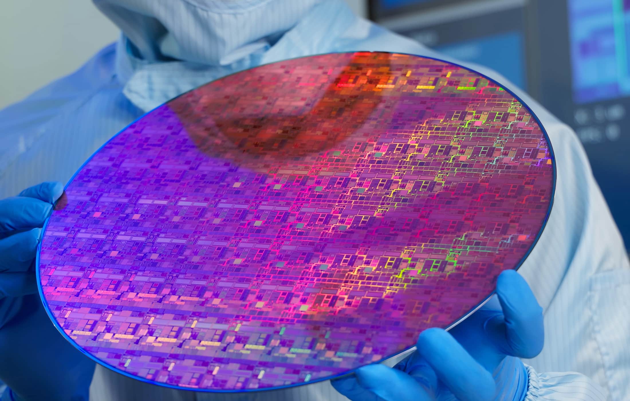
Fabrication: Full 300 mm semiconductor foundry processes, with progressively tighter integration between qubit devices and classical control electronics. Diraq/imec’s landmark October 2025 result demonstrated >99% gate fidelities in silicon spin qubits fabricated on 300 mm foundry wafers — the first time foundry-manufactured qubits crossed the fault-tolerance threshold.
Strengths:
This approach represents the most direct path to the silicon scaling vision: millions of qubits on a chip, manufactured using existing semiconductor fabs. The Diraq/imec result proved that foundry fabrication and fault-tolerance-level fidelity are not mutually exclusive — a question that had been open until October 2025. Detailed error characterisation via gate-set tomography identified residual ²⁹Si nuclear spin noise as the dominant error source, which is addressable through further isotopic purification. The approach also enables co-integration of qubits with cryo-CMOS control electronics, potentially solving the wiring bottleneck that limits all platforms at scale.
Weaknesses:
The results are still from small devices — pairs of qubits, not arrays. Maintaining high fidelity across large arrays (hundreds to thousands of dots) has not been demonstrated in a foundry setting. Variability between qubits on a wafer, while better than feared, still requires per-qubit calibration that becomes impractical at scale without automated tuning. The two-qubit fidelities (~99–99.5%) are above threshold but below what donors achieve, leaving less margin for error correction overhead.
The bet: The semiconductor industry’s existing capability — mature processes, massive investment, global supply chains — is an asset so powerful that it’s worth accepting somewhat lower qubit quality in exchange for manufacturing scalability. Performance will converge as foundry processes are optimized specifically for qubits.
How They Compare
| Dimension | Donor Qubits | Quantum Dots | Foundry-Compatible |
|---|---|---|---|
| Best 2Q gate fidelity | 99.9% (SQC) | 99.5% (RIKEN/QuTech) | 99–99.5% (Diraq/imec) |
| Best 1Q gate fidelity | 99.99% (SQC) | 99.8% (RIKEN) | 99.85% (Diraq) |
| Coherence times | Seconds (nuclear) | 10–100 μs (electron) | 10–100 μs (electron) |
| Max qubit count | 11 (SQC) | 12 (Intel) | 2 (Diraq/imec) |
| Fabrication method | STM lithography | E-beam/optical litho | 300 mm foundry |
| Devices per wafer | ~1 (bespoke) | ~24,000 (Intel) | ~24,000+ (foundry) |
| Logical operations? | Yes (SZIQA) | No | No |
| Error correction? | Error detection (SZIQA) | Phase-flip code (RIKEN) | No |
| CMOS integration? | Limited | In development | Native |
The table makes the tradeoff clear: donor qubits lead on performance and have demonstrated the most advanced operations, but face the steepest manufacturing challenge. Foundry-compatible devices lead on manufacturability but have demonstrated the fewest qubits and the least complex operations. Gate-defined quantum dots sit between the two, with moderate performance and moderate fabrication scalability.
Will They Converge?
The most important question for the field is not which approach will win, but whether the approaches will converge — whether the performance of foundry-manufactured qubits will rise to meet the fidelity of donor qubits, or whether donor fabrication will become scalable enough to compete with foundries.
There are reasons for optimism on both fronts. The Diraq/imec result showed that the dominant error source in foundry qubits is ²⁹Si nuclear spin noise — a problem with a known solution (isotopic purification). If foundries can source enriched ²⁸Si substrates at scale, a significant chunk of the fidelity gap closes. On the donor side, SQC has explicitly discussed scaling through modular arrays of donor clusters connected by exchange coupling — a strategy that trades atomic-precision placement of every individual atom for a more structured, repeatable architecture.
There is also a hybrid possibility: donor clusters used as high-fidelity logical qubit nodes, connected by quantum-dot-style exchange links fabricated with conventional lithography. This would combine the donor approach’s performance advantage with the quantum dot approach’s fabrication scalability. It is speculative, but the physics does not obviously forbid it.
What is clear is that silicon quantum computing is not a single horse in the quantum computing race — it is a stable. And the diversity of approaches within the platform may ultimately be one of its greatest strengths: if any one of the three paths reaches fault-tolerant operation, the others provide the manufacturing knowledge, the control techniques, or the error correction protocols needed to scale it.
Quantum Upside & Quantum Risk - Handled
My company - Applied Quantum - helps governments, enterprises, and investors prepare for both the upside and the risk of quantum technologies. We deliver concise board and investor briefings; demystify quantum computing, sensing, and communications; craft national and corporate strategies to capture advantage; and turn plans into delivery. We help you mitigate the quantum risk by executing crypto‑inventory, crypto‑agility implementation, PQC migration, and broader defenses against the quantum threat. We run vendor due diligence, proof‑of‑value pilots, standards and policy alignment, workforce training, and procurement support, then oversee implementation across your organization. Contact me if you want help.
Related Content