The Foundry’s Hidden Supply Chain: Who Really Wins If Silicon Spin Quantum Computing Wins

Table of Contents
In September 2025, a team from the Australian startup Diraq and Belgium’s imec published a result in Nature that no one in the semiconductor industry could ignore. They had fabricated silicon quantum dot spin qubits on imec’s industrial 300-millimeter wafer line – the same kind of manufacturing platform that produces billions of classical processors every year – and achieved two-qubit gate fidelities consistently exceeding 99%. Not on a single heroic device selected from hundreds. On randomly chosen chips, pulled at random from the production run.
Three months later, Silicon Quantum Computing (SQC), an Australian company founded by physicist Michelle Simmons, published its own Nature paper demonstrating an 11-qubit, multi-register processor with fidelities reaching 99.99% – and, remarkably, performance that improved as more qubits were added. In London, Quantum Motion delivered the industry’s first full-stack quantum computer built on standard CMOS fabrication to the UK’s National Quantum Computing Centre. And in a Malibu cleanroom owned jointly by Boeing and General Motors, HRL Laboratories continued refining the encoded spin qubit approach it had pioneered in silicon-germanium heterostructures, publishing two-dimensional qubit arrays with multilevel interconnects.
Something had shifted. For years, silicon spin qubits occupied a peculiar position in the quantum computing landscape: universally acknowledged as the most scalable approach in theory, yet perpetually dismissed as the most immature in practice. Superconducting qubits had Google and IBM racing past a thousand physical qubits. Trapped ions had Quantinuum demonstrating logical circuits. Neutral atoms had QuEra and PASQAL reaching thousands of qubits in reconfigurable arrays. Silicon spin had… a handful of qubits, impressive coherence times, and a promissory note.
That promissory note reads: if you can make a qubit out of a transistor, you inherit six decades of semiconductor manufacturing infrastructure – the most powerful industrial machine civilization has ever built.
In 2025, the first credible evidence arrived that the note might be honored. And the supply chain implications are unlike any other modality, because the silicon spin supply chain is, to a first approximation, the semiconductor supply chain – a $600 billion global industrial ecosystem already optimized for volume, yield, and relentless miniaturization. The question is no longer whether silicon can host competitive qubits. It’s whether the additional ingredients this modality demands – isotopically purified silicon-28, cryogenic control electronics, and fabrication processes tuned for quantum rather than classical performance – can be produced at the scale and quality the quantum industry will require.
This article maps that supply chain: from the isotopically enriched substrates to the foundry processes, from the cryogenic control chips to the dilution refrigerators (yes, silicon spin still needs cold, just not as cold), from the control electronics to the classical computing integration layer. At each point, we identify the key players, the bottlenecks, and the strategic implications for investors, technology executives, and policymakers asking: if silicon spin wins, who else wins?
This analysis examines technology and market dynamics. It does not constitute financial or investment advice.
Anatomy of a Silicon Spin Quantum Computer
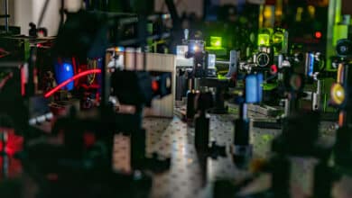
If the superconducting quantum computer is defined by its chandelier-shaped dilution refrigerator and the neutral-atom system by its camera image of fluorescent dots, the silicon spin quantum computer is defined by… a chip. A chip that looks, to the untrained eye, remarkably like the processors in your laptop or phone. That’s the point.
A silicon spin qubit stores quantum information in the spin – the intrinsic angular momentum – of a single electron (or hole) trapped in a tiny electrically defined cage called a quantum dot. The quantum dot is formed by applying precise voltages to metal gate electrodes patterned on top of a silicon substrate, creating an electrostatic potential well roughly 30 to 100 nanometers across. Within that well, a single electron’s spin points either “up” or “down” – the quantum analogue of a classical bit’s 0 or 1 – and can be placed in superpositions of both states simultaneously. Two neighboring quantum dots can be made to interact through their exchange coupling, enabling two-qubit entangling gates.
There are several distinct sub-approaches within the silicon spin family, each with different fabrication requirements and supply chain implications:
Gate-defined quantum dots – the dominant approach – use electrostatic gates on silicon metal-oxide-semiconductor (MOS) structures or silicon-germanium (Si/SiGe) heterostructures to trap electrons. This is the path pursued by Diraq, Quantum Motion, Intel, Quobly, SemiQon, and imec. The fabrication is closest to standard CMOS transistor manufacturing. Donor-based qubits use individual phosphorus atoms implanted into silicon with atomic precision, encoding quantum information in the nuclear and electron spins of the donor atoms. This is SQC’s approach, pioneered over 25 years by Michelle Simmons at UNSW Sydney. The fabrication uses scanning tunneling microscope (STM) lithography to place atoms with sub-nanometer accuracy – a radically different manufacturing paradigm from CMOS. Encoded spin qubits use three or more electron spins in multi-dot configurations to define qubit states that are inherently protected against certain types of noise. HRL Laboratories has demonstrated universal control of encoded qubits in Si/SiGe, using only voltage pulses rather than microwaves for gate operations.
A complete silicon spin quantum computing system requires, at minimum:
A quantum processor chip (QPU) fabricated on isotopically enriched silicon-28, with quantum dot structures defined by nanoscale gate electrodes. A dilution refrigerator or cryogenic cooling system – silicon spin qubits typically operate between 10 millikelvin and 1 kelvin, depending on the approach. Diraq has demonstrated operation above 1 K, which substantially relaxes cryogenic requirements compared to superconducting qubits. Cryogenic control electronics – classical circuits, increasingly co-integrated on the same chip or at least within the same cryostat, that generate the voltage pulses and microwave signals used to control qubits and read out their states. Room-temperature control infrastructure – arbitrary waveform generators, FPGA-based real-time controllers, and signal processing equipment. Classical computing infrastructure — for calibration, error correction decoding, and hybrid quantum-classical workflows. Software and middleware – compilers, optimizers, and the orchestration layer.
Two features distinguish this stack from every other quantum computing modality. First, the QPU fabrication can – at least in principle – be done in existing semiconductor foundries, using processes derived from those already running at massive scale. Second, the control electronics can – at least in principle – be co-integrated with the qubits on the same chip, eliminating the cabling bottleneck that constrains every other modality. Both of these principles remain works in progress. But the progress in 2025 was substantial enough to demand serious analysis of the supply chain that would support them at scale.
The Silicon-28 Imperative: Quantum Computing’s Purest Ingredient
Every silicon spin qubit shares one non-negotiable material requirement: the silicon it lives in must be isotopically purified.
Natural silicon is composed of three isotopes: silicon-28 (92.2%), silicon-29 (4.7%), and silicon-30 (3.1%). Silicon-28 and silicon-30 are spin-free – magnetically silent. Silicon-29 carries a nuclear spin of ½, and those randomly distributed magnetic moments act like microscopic compass needles, creating a fluctuating magnetic noise environment that destroys the delicate quantum states of spin qubits. The effect is devastating. In natural silicon, qubit coherence times are measured in microseconds. In silicon enriched to 99.99% silicon-28, coherence times extend to milliseconds or longer – an improvement of three orders of magnitude.
Isotopically enriched silicon-28 is therefore not a performance optimization for silicon spin qubits. It is a prerequisite.
The historical supply chain for this material is a legacy of metrology, not computing. The most famous source of ultra-pure silicon-28 was the Avogadro Project – an international effort to redefine the kilogram by manufacturing a nearly perfect sphere of isotopically pure silicon. That project, completed in the 2010s, produced kilogram-scale quantities of silicon-28 enriched to 99.9984%, with residual silicon-29 below 50 parts per million. The enrichment was done using gas centrifuge cascades processing silicon tetrafluoride (SiF₄), a technique borrowed from uranium enrichment – and historically concentrated in Russia.
For quantum computing, this supply chain is wholly inadequate. The quantities are tiny (kilograms, not tonnes), the suppliers are few, the processes are bespoke, and the geopolitical concentration (Russia was the primary enrichment source) is unacceptable for a technology with national security implications.
Enter ASP Isotopes (NASDAQ: ASPI), a South Africa-based advanced materials company that in March 2025 commenced commercial production of enriched silicon-28 at its second enrichment facility in Pretoria. ASP’s proprietary Aerodynamic Separation Process directly enriches silane (SiH₄) gas, avoiding the additional chemical conversion steps required by competitors processing silicon tetrafluoride. The company has secured multiple supply agreements with U.S.-based customers – including what it described as its largest silicon-28 contract to date in September 2025, with deliveries beginning in Q1 2026. ASP’s facility has demonstrated annual capacity exceeding 80 kilograms of silicon-28 enriched to at least 99.995%, surpassing earlier guidance of 50 kilograms.
In Australia, Silex Systems uses laser-based isotope separation technology to produce silicon-28, supporting SQC’s domestic supply chain. This arrangement gives Australia a notable strategic advantage: the entire value chain from raw material to finished quantum chip can remain within sovereign control – a fact not lost on the Australian government’s defence and technology planners.
Other emerging sources include research-scale suppliers like NIST in the United States and various academic institutions, but none yet operate at commercial volumes. The historical Russian supplier, Isotope JSC, remains technically capable but is increasingly inaccessible due to geopolitical constraints.
The material itself, however, is only part of the challenge. Quantum chips use thin epitaxial layers of enriched silicon-28 – typically 100 nanometers to 1 micrometer thick – grown on standard silicon substrates via chemical vapor deposition (CVD). This epitaxial growth must achieve extraordinary uniformity: if the concentration of residual silicon-29 varies across the wafer, different qubits will have different coherence properties, requiring different calibration strategies for each one. Imec’s 300-millimeter spin qubit platform has demonstrated the required uniformity, but the supply chain for isotopically enriched epitaxial wafers at 300 mm scale remains in its infancy.
The investor read: Isotopically enriched silicon-28 is the helium-3 of the silicon spin modality – a material so specialized that its supply chain barely exists at commercial scale. ASP Isotopes is the most visible pure-play opportunity, with a publicly traded stock and a near-billion-dollar market capitalization built largely on the promise of quantum-grade silicon demand. But unlike helium-3, silicon-28 enrichment can be scaled using established isotope separation physics, and the material is not consumed during operation (unlike helium-3 in dilution refrigerators, which must be continuously recirculated). The structural constraint is not geological scarcity but industrial readiness: the transition from kilogram-scale research supply to tonne-scale commercial production has not yet occurred. Companies that secure reliable, high-purity silicon-28 supply — or that develop alternative enrichment pathways – occupy a strategic chokepoint in the silicon spin supply chain.
The Foundry Advantage: Why Silicon Spin’s Supply Chain Is Hiding in Plain Sight
The defining proposition of silicon spin quantum computing is that qubits can be fabricated in the same factories, using the same processes, that produce classical microprocessors. This is both the modality’s greatest strength and its most commonly overstated claim.
The strength is real. Gate-defined silicon spin qubits are, at their core, modified transistors. The quantum dot is a transistor with one electron. The gate electrode stack – metal gates on a thin oxide layer over a silicon channel – is fabricated using lithography, deposition, and etching techniques that exist at industrial scale in every major semiconductor foundry. When Quantum Motion delivered the first full-stack CMOS quantum computer in September 2025, it used QPUs fabricated on standard 300-millimeter silicon wafers at a commercial chip foundry. When Diraq and imec demonstrated above-99% fidelity on industrial wafers, they used imec’s existing 300-millimeter process flow, optimized over nearly a decade for quantum dot structures.
But the overstated version – that you can simply repurpose an existing CMOS fab line to make quantum processors – misses critical nuances. The fabrication processes must be modified in specific ways:
The silicon channel must be isotopically enriched silicon-28, requiring custom epitaxial growth. The gate oxide must be extraordinarily clean – interface defects at the silicon-oxide boundary are a primary source of charge noise that disrupts qubits. Imec’s process optimization has reduced this noise dramatically, but it required years of careful engineering beyond what standard logic processes demand. The gate dimensions and spacing must be precisely controlled to define quantum dots at the nanometer scale, and the pitch between dots determines qubit coupling strengths. Standard deep-UV lithography works, but extreme ultraviolet (EUV) lithography – demonstrated by imec for quantum dot gates at IEDM 2025 – offers the overlay accuracy and yield advantages needed for larger arrays. The thermal budget during fabrication must be carefully managed to preserve isotopic enrichment and minimize defect introduction.
Despite these modifications, the key players in this layer are drawn from the existing semiconductor ecosystem:
Imec (Belgium) operates the most advanced publicly accessible spin qubit fabrication platform in the world. Its 300-millimeter process flow for MOS-based quantum dot structures has enabled Diraq’s fidelity breakthroughs and continues to refine overlapping-gate and single-layer-gate architectures. Imec’s role in the silicon spin supply chain is analogous to what TSMC is for advanced logic: the research and process development engine that translates qubit designs into manufacturable devices. Its demonstration of EUV lithography for quantum dot fabrication at IEDM 2025 was a landmark – it means spin qubit arrays can now be printed on full 300-millimeter wafers with the same tools used for the most advanced classical chips.
Intel brings the largest semiconductor manufacturing footprint of any company pursuing silicon spin qubits. Its Tunnel Falls 12-qubit chip, fabricated on Intel’s 300-millimeter production line using advanced transistor techniques including EUV lithography, was released to the research community in late 2024 through the Laboratory for Physical Sciences’ Qubits for Computing Foundry (QCF) program. Intel’s strategic advantage is institutional: decades of process control, defect engineering, and high-volume manufacturing discipline. Its strategic disadvantage is pace – as of early 2026, Intel’s largest demonstrated chip has 12 physical qubits, and no logical qubit has been demonstrated, putting it behind peers in qubit count if not in manufacturing sophistication.
STMicroelectronics (France/Italy) has partnered with Quobly to adapt its 28-nanometer Fully Depleted Silicon-on-Insulator (FD-SOI) process at its Crolles fabrication facility near Grenoble for quantum processor production. This is strategically significant: ST is one of the world’s largest semiconductor companies, and its FD-SOI technology is already used in automotive, IoT, and wireless applications. Quobly’s bet is that the FD-SOI platform – with its built-in back-gate control and proven scalability – is the optimal substrate for co-integrating qubits and cryogenic control electronics on the same chip. The partnership was announced in late 2024, with first results expected in 2026 and commercial QPU production targeted for 2027.
GlobalFoundries (U.S.) is a manufacturing partner for Diraq, providing another pathway to high-volume quantum chip fabrication alongside imec. The involvement of multiple foundry partners reflects Diraq’s strategy of using the semiconductor industry’s existing capacity rather than building bespoke facilities.
SkyWater Technology (U.S., NASDAQ: SKYT) has partnered with SQC to advance hybrid quantum-classical computing. SkyWater’s role is to provide superconducting resonators and tailored silicon wafers from its secure production line – emphasizing trusted supply chain integrity for defense and government applications. SkyWater also collaborates with QuamCore on digital superconducting controllers for quantum systems, making it a multi-modality player in the quantum fabrication ecosystem.
The donor-based approach pursued by SQC represents a fundamentally different fabrication paradigm. SQC does not use photolithography. Instead, it places individual phosphorus atoms into silicon using scanning tunneling microscope (STM) lithography – a process with 0.13-nanometer (atomic-level) precision that SQC claims is the most accurate semiconductor manufacturing process in the world. In November 2025, SQC demonstrated the ability to pattern 250,000 qubit registers in just eight hours, addressing concerns about manufacturing throughput. SQC is the only private quantum computing company that manufactures its own QPUs end-to-end – a full-stack vertical integration model that contrasts sharply with the foundry-based approaches of Diraq, Quantum Motion, and Quobly.
The investor read: The foundry layer is where silicon spin’s investment thesis differs most profoundly from every other modality. In superconducting, photonic, or trapped-ion quantum computing, QPU fabrication is either in-house (requiring massive capital expenditure) or handled by a small number of specialized facilities. In silicon spin, the fabrication infrastructure already exists – in the form of the $600 billion global semiconductor industry. This doesn’t mean quantum chips will be cheap or easy to make. It means the capital expenditure barrier to scaling fabrication is dramatically lower than for competing modalities. The companies positioned to capture value in this layer fall into two categories: foundry partners that offer quantum-specific process development as a service (imec, GlobalFoundries, ST) and full-stack companies that control their own fabrication (SQC, Intel). For investors, the foundry model offers exposure to silicon spin without betting on a single quantum computer maker — analogous to investing in TSMC rather than picking between Apple and Nvidia.
The Cryogenics Question: Cold, but Not That Cold
Silicon spin qubits need to be cold. But the question of how cold is one of the modality’s most consequential variables – and it divides the field.
Most gate-defined silicon spin qubits today operate at temperatures between 10 and 100 millikelvin, requiring dilution refrigerators similar to those used for superconducting qubits. This means the silicon spin supply chain shares the same cryogenic dependency – Bluefors, Oxford Instruments, Leiden Cryogenics, Maybell Quantum – and the same helium-3 constraints described in our superconducting ecosystem analysis. When Quantum Motion delivered its system to the UK’s NQCC, it included a dilution refrigerator and integrated control electronics housed in three standard server racks.
But here is where silicon spin diverges from superconducting in a strategically important way. Multiple groups have demonstrated silicon spin qubit operation above 1 kelvin – a temperature achievable with much simpler, cheaper, and more readily available cryocoolers rather than dilution refrigerators. In 2024, Diraq published results in Nature showing qubit operation above 1 K with single-qubit Clifford gate fidelities up to 99.85% and two-qubit gates approaching 99%. SQC has published record qubit readout fidelities at elevated temperatures. The operational significance is substantial: at 1 K, the available cooling power is roughly a thousand times greater than at 10 millikelvin, and the cooling hardware is orders of magnitude cheaper and more compact.
This “hot qubit” capability has direct supply chain implications. If silicon spin systems can operate at 1 K or above, the cryogenic supply chain shifts from dilution refrigerators (a market dominated by fewer than five companies, with six-to-nine-month lead times and prices exceeding $500,000 per unit) to Gifford-McMahon or pulse tube cryocoolers (a broader, more competitive market with established industrial supply chains serving MRI, semiconductor, and defense applications). The heat budget at 1 K also makes it far more practical to co-locate classical control electronics with qubits inside the cryostat – a critical enabler for scalability.
Not all silicon spin approaches can operate at elevated temperatures. The donor-based qubits used by SQC still require millikelvin temperatures for optimal performance, as do most Si/SiGe heterostructure systems. The hot-qubit advantage is most pronounced for MOS-based quantum dot qubits – the approach pursued by Diraq and Quantum Motion.
The investor read: The cryogenics layer is where silicon spin’s supply chain story gets interesting. In the near term, the modality shares superconducting’s dependence on dilution refrigerators and helium-3, and investors evaluating silicon spin companies should apply the same supply chain risk analysis. But in the medium term, the demonstrated path to 1 K operation creates a potential escape from the cryogenic bottleneck – one that no other gate-based modality can currently match. Companies developing silicon spin systems that operate above 1 K effectively decouple themselves from the most constrained layer of the quantum supply chain. This is a differentiated risk profile that merits attention.
Cryo-CMOS: The Control Electronics That Change Everything
Every quantum computing modality faces a wiring problem. As qubit counts grow, the number of control and readout lines connecting the cold quantum processor to room-temperature electronics grows proportionally – and each wire carries heat into the cryostat, eventually overwhelming its cooling capacity. In superconducting quantum computers, this wiring bottleneck is already a binding constraint at a few hundred qubits.
Silicon spin qubits have a unique answer: put the control electronics on the same chip as the qubits.
Because spin qubits are fabricated using CMOS-compatible processes, the classical transistors needed to control them can – in principle – be fabricated alongside them, creating a monolithic quantum-classical integrated circuit. This co-integration would eliminate most external wiring, dramatically reduce heat load, and enable the dense qubit arrays (millions of qubits per chip) that the silicon spin modality promises.
The practical challenge is that CMOS transistors behave differently at cryogenic temperatures. Threshold voltages shift, carrier mobilities change, noise characteristics transform, and thermal management becomes radically more constrained. Designing circuits that function reliably at millikelvin or 1 K temperatures requires specialized knowledge that sits at the intersection of quantum physics and chip design.
Several companies are building this capability:
Quobly (France) and CEA-Leti are the most advanced in co-integration. At ISSCC 2025, they presented a cryo-CMOS charge readout circuit achieving just 18.5 microwatts per qubit – a tenfold reduction over prior art – fabricated in FD-SOI technology. The circuit uses quadrature amplitude modulation (QAM) to read out multiple qubits through a single amplifier, directly addressing the wiring bottleneck. Combined with Quobly’s strategy of building both qubits and control electronics in FD-SOI, this represents the clearest path to fully integrated quantum-classical chips. Quobly targets a 100-qubit chip by 2026 and a million physical qubits by 2031.
SemiQon (Finland), a VTT Technical Research Centre spinout, has taken a different approach: rather than adapting room-temperature CMOS for cryogenic use, SemiQon designs transistors from the ground up for cryogenic operation. Its cryo-CMOS transistors, launched in late 2024, consume 0.1% of the power and deliver heat dissipation levels 1,000 times lower than conventional transistors at cryogenic temperatures. SemiQon has secured approximately €24 million in total funding, including €17.5 million from the European Innovation Council in 2025, and positions itself as a component supplier – providing cryo-optimized chips and quantum dot devices to quantum computer builders, rather than building complete systems. The company operates from VTT’s Micronova pilot line in Espoo and has entered into a collaboration with imec to accelerate industrial readiness.
Intel’s Horse Ridge and Pando Tree cryogenic control chips represent the largest company’s bet on this approach. Horse Ridge, fabricated in Intel’s 22-nanometer FinFET process, was demonstrated operating at 4 K and controlling multiple qubits simultaneously. The successor Pando Tree chip further increases channel count and integration density. Intel’s vision is a fully integrated system where qubit arrays and control ASICs coexist in the same cryogenic package, connected by silicon interposers rather than coaxial cables.
SEEQC (U.S.), while primarily associated with superconducting quantum computing, develops Single Flux Quantum (SFQ) cryogenic control technology that is modality-agnostic – its digital superconducting logic can control both superconducting and spin qubits at millikelvin temperatures. SEEQC’s partnership with Taiwan’s ITRI for manufacturing SFQ chips adds a semiconductor fabrication dimension to the cryogenic control landscape.
The broader control electronics ecosystem – Zurich Instruments, Qblox, Quantum Machines, Keysight Technologies – also serves silicon spin systems with room-temperature equipment. Qblox has an active collaboration with Bluefors specifically targeting spin qubit systems, and HRL Laboratories’ open-source spinQICK platform provides FPGA-based control solutions specifically designed for solid-state spin qubits.
The investor read: Cryo-CMOS is arguably the most strategically important supply chain layer for silicon spin quantum computing, because it is what transforms the modality’s theoretical scalability advantage into a practical engineering reality. Without cryogenic control co-integration, silicon spin faces the same wiring bottleneck as superconducting – and loses its primary differentiator. The companies building this capability (Quobly/CEA-Leti, SemiQon, Intel) are therefore foundational to the silicon spin value proposition. SemiQon’s component-supplier model is particularly interesting: rather than betting on a single full-stack quantum computer maker, SemiQon sells into the entire silicon spin ecosystem, positioning itself as a picks-and-shovels play on the modality. The cryo-CMOS market is also relevant beyond quantum computing – cryogenic electronics have applications in space, defense, and high-performance computing – providing potential revenue diversification.
The Company Landscape: Two Continents, Two Philosophies
The silicon spin quantum computing ecosystem is geographically concentrated in two clusters – Australia and Europe – with the United States contributing through corporate R&D labs rather than venture-backed startups. The companies within these clusters divide along a philosophical fault line: those pursuing CMOS-compatible gate-defined quantum dots (which prioritize manufacturing scalability) and those pursuing atom-precise donor-based qubits (which prioritize qubit quality and simplicity of error correction).
The CMOS Camp
Diraq (Sydney, Australia) is the most aggressively commercializing CMOS spin qubit company. Founded in 2022 by Andrew Dzurak – who led the team that built the first silicon quantum logic gate in 2015 – Diraq has raised over US$150 million including government funding, with a Series B planned for later in 2026. The company’s roadmap targets its first commercial quantum computer by 2029 and one million qubits on a single chip by 2031, with projected manufacturing costs below one dollar per qubit. Diraq has been selected for Stage B of DARPA’s Quantum Benchmarking Initiative (QBI) – one of only 11 companies to advance – and has partnerships with imec, GlobalFoundries, Nvidia, and Dell. Its qubits operate above 1 K, reducing cryogenic requirements, and it has demonstrated cryo-CMOS control chip co-integration in partnership with the University of Sydney’s Emergence Quantum group. Diraq’s most recent acquisition of assets from SQC’s competitor program suggests consolidation in Australia’s silicon qubit ecosystem.
Quantum Motion (London, UK) delivered the first full-stack silicon CMOS quantum computer in September 2025, fabricated using standard 300-millimeter wafer technology. The company has raised over £62 million, including a Series B led by Bosch and Porsche, and employs over 100 staff across the UK, US, Australia, and Spain. Quantum Motion’s QPU uses a tile-based architecture designed to scale to millions of qubits per chip through repeatable printing of compute, readout, and control elements. The company was also selected for DARPA QBI Stage B and leads the SiQEC (Silicon Quantum Error Correction) project with UCL, aiming to demonstrate repeated error correction cycles on a spin qubit platform.
Quobly (Grenoble, France) emerges from 15 years of collaborative research between CEA-Leti and CNRS. Co-founded by Maud Vinet and Tristan Meunier, Quobly has raised approximately €40 million (a €19 million record European seed round in 2023, plus €21 million in 2025) and holds about 40 patents. Its strategic differentiator is the partnership with STMicroelectronics for FD-SOI fabrication – giving it direct access to one of Europe’s most advanced semiconductor manufacturing lines. Quobly is surrounded by a uniquely integrated European ecosystem: CEA-Leti for process R&D, STMicroelectronics for manufacturing, CNRS for fundamental physics, and TNO for materials characterization. The company targets a 100-qubit chip by 2026 and a million physical qubits by 2031.
SemiQon (Espoo, Finland) occupies a distinct niche as a component supplier rather than a full-stack quantum computer maker. Its cryo-CMOS transistors and quantum dot chips are designed to be sold to other quantum computer builders – a business model analogous to how ARM licenses processor designs rather than making phones. SemiQon has raised approximately €24 million and operates from VTT’s Micronova facility.
Intel (Santa Clara, U.S.) brings unmatched semiconductor manufacturing capability but has been more deliberate in its quantum roadmap. Its 12-qubit Tunnel Falls chip serves primarily as a research vehicle distributed through the QCF program. Intel’s long-term vision encompasses fully integrated qubit-plus-control chips, leveraging its 300-millimeter fabs and advanced packaging technology. But unlike the startups, Intel treats quantum as one program among many – and has yet to commit the focused investment that would signal a full-scale commercialization push.
HRL Laboratories (Malibu, U.S.) is privately held by Boeing and General Motors, pursuing Si/SiGe encoded spin qubits with government (primarily DARPA and DOD) funding. HRL’s research output is world-class – its 2023 demonstration of universal logic with encoded qubits in Nature was a landmark – but its commercial pathway runs through defense applications rather than the commercial cloud computing market targeted by most competitors.
The Atomic-Precision Camp
Silicon Quantum Computing (Sydney, Australia), founded by Michelle Simmons in 2017, stands apart. SQC places individual phosphorus atoms into silicon with 0.13-nanometer precision using STM lithography – a radically different manufacturing approach that produces what the company claims are the highest-fidelity qubits in any material. SQC’s 14|15 architecture (named for the number of phosphorus atoms in its two multi-nuclear spin registers) achieved up to 99.99% fidelity in its December 2025 Nature paper, and the company demonstrated Grover’s algorithm at 98.9% accuracy without any error correction — suggesting that its qubits may require far less error correction overhead than competing approaches.
SQC has progressed to DARPA QBI Stage B, sells quantum machine learning processors (“Watermelon”) to the Commonwealth Bank of Australia and the Australian Department of Defence, and launched “Quantum Twins” – application-specific quantum simulators for materials discovery – in February 2026. The company recently demonstrated the ability to pattern 250,000 qubit registers in eight hours, addressing manufacturing throughput concerns. Its partnership with SkyWater Technology provides a pathway to U.S.-based trusted manufacturing.
SQC’s model is the most vertically integrated in the silicon spin space: it designs, fabricates, and tests new quantum chips in under a week, using its own atomic-precision manufacturing process. This is a fundamentally different supply chain from the foundry-based model – with correspondingly different risk profiles and scaling dynamics.
The “If Silicon Spin Wins” Analysis: Who Else Wins?
If silicon spin quantum computing achieves commercial scale, the ripple effects through adjacent industries would be distinctive – because many of the “winners” are companies that already dominate the classical semiconductor ecosystem.
The Semiconductor Foundry Ecosystem
The most direct beneficiaries of a silicon spin victory would be the semiconductor foundries and their equipment suppliers. If quantum chips can be manufactured on 300-millimeter CMOS lines, then every major foundry becomes a potential quantum chip manufacturer – and the enormous capital investments already made in semiconductor fabrication infrastructure become dual-use assets.
Equipment companies like ASML (EUV lithography), Applied Materials (deposition and etch), Lam Research (etch and deposition), KLA Corporation (metrology and inspection), and Tokyo Electron (various process tools) would see incremental demand as quantum-specific process modules are developed. The volumes would be tiny compared to logic and memory fabrication – but the margin on quantum-grade processing could be substantial, and the R&D relationships would position these companies for future growth.
Foundries that develop quantum-specific process capabilities – imec, GlobalFoundries, STMicroelectronics, SkyWater, and potentially TSMC and Samsung – would capture direct revenue from quantum chip fabrication. This creates an intriguing dynamic: the foundry model that has driven classical semiconductor scaling for decades could be extended to quantum, with the same foundry customers (now quantum computer companies) sending designs to the same manufacturing partners.
The Isotope Enrichment Industry
ASP Isotopes is the most obvious beneficiary, as the leading commercial supplier of enriched silicon-28. But the broader isotope separation industry – including companies and national laboratories with centrifuge, laser separation, or aerodynamic separation capabilities – would see growing demand. The market for isotopically enriched silicon is currently tiny (tens of millions of dollars at most) but could grow by one to two orders of magnitude if silicon spin achieves manufacturing scale.
The Cryogenics Industry (With a Caveat)
Silicon spin’s relationship with the cryogenics industry is more nuanced than superconducting’s. In the near term, the same companies benefit: Bluefors, Oxford Instruments, Leiden Cryogenics, Maybell Quantum, and Kiutra would supply dilution refrigerators for silicon spin systems operating at millikelvin temperatures. But if the hot-qubit path (above 1 K) proves viable for commercial systems, the dependency shifts toward simpler cryocooler technology – a market where companies like Sumitomo Heavy Industries, Cryomech (now part of Bluefors), and Edwards Vacuum have established positions. The net effect could be to broaden the cryogenic supply chain rather than concentrate it.
Classical Computing and AI
Silicon spin quantum computing generates an unusual demand for classical AI and machine learning – not as a quantum application, but as a manufacturing tool. The calibration and tuning of quantum dot arrays is extraordinarily complex: each qubit requires precise voltage adjustments to its gate electrodes, and the optimal settings interact nonlinearly across the array. Quantum Motion, Diraq, and others have reported using machine learning algorithms to automate this tuning process – and as qubit counts grow, the classical computing demands for calibration may become substantial.
Nvidia has partnered with both Diraq and SQC, reflecting recognition that quantum-classical integration will require GPU-accelerated workflows. Dell has partnered with Diraq on system integration. These partnerships suggest that the quantum computing supply chain increasingly includes classical computing giants as essential infrastructure providers.
What Silicon Spin Means for Quantum Threat Timelines
For CISOs and security architects, the silicon spin supply chain analysis has a specific and uncomfortable implication.
The other quantum computing modalities face supply chain bottlenecks that function as natural brakes on scaling. There are only a handful of companies that can build dilution refrigerators. There are only a few foundries that can fabricate ion trap chips. The laser systems for neutral atoms are specialized and capacity-constrained. These bottlenecks don’t prevent progress, but they impose a pace that is fundamentally limited by industrial capacity.
Silicon spin’s supply chain, if the CMOS-compatible approach proves out, faces far fewer such brakes. The manufacturing infrastructure already exists at enormous scale. The talent pool for semiconductor process engineering is orders of magnitude larger than for cryogenics or precision optics. The capital investment required to scale production is a rounding error in the semiconductor industry’s annual equipment spending.
This doesn’t mean silicon spin will reach cryptanalytically relevant quantum computer (CRQC) capability first – the modality remains behind in demonstrated qubit counts. But it means that if silicon spin crosses the threshold from research curiosity to engineering reality (as the 2025 results suggest it might), the subsequent scaling could be faster than for any competing modality. The semiconductor industry’s scaling machine, once engaged, operates at a velocity that no bespoke quantum manufacturing process can match.
This warrants monitoring. Organizations implementing post-quantum cryptography should factor silicon spin’s progress into their threat timeline models – not because it changes the immediate urgency (that urgency already exists), but because it could compress the timeline between “promising modality” and “operational threat” more than current models assume.
Sovereign Ecosystems and the Geography of Silicon Spin
The silicon spin quantum computing ecosystem has a distinctive geography that differs markedly from superconducting or trapped ions.
Australia has built the deepest national capability in silicon spin qubits. Two globally competitive companies (SQC and Diraq), world-class university research programs (UNSW, University of Sydney, University of Melbourne), domestic isotope enrichment capability (Silex Systems), and active government investment through the National Reconstruction Fund and defence procurement create an ecosystem with genuine end-to-end quantum sovereignty. Australia’s challenge is scale: the domestic market is small, and both SQC and Diraq are expanding internationally (primarily to the U.S.) to access larger customer bases and talent pools.
Europe has a fragmented but collectively formidable position. Quobly anchors the French ecosystem (with CEA-Leti, CNRS, and STMicroelectronics). Quantum Motion leads in the UK (with NQCC and UCL). SemiQon and VTT strengthen Finland’s position. Imec provides the continent’s manufacturing R&D backbone. And QuTech in the Netherlands, while focused on research, has produced some of the highest-fidelity germanium spin qubit results in the world. The European Quantum Pilot Line initiative connects several of these nodes. Europe’s advantage is the integration between national labs, foundries, and startups – the kind of institutional fabric that China has sought to replicate through top-down investment.
The United States has significant corporate R&D (Intel, HRL Laboratories) and academic programs (Princeton, University of Wisconsin-Madison, University of Rochester, Sandia National Laboratories), but has notably fewer venture-backed silicon spin startups than Australia or Europe. The DARPA QBI program is an important catalyst, and Intel’s QCF distribution of Tunnel Falls chips to U.S. research labs is building ecosystem capacity. But the most commercially advanced silicon spin companies are headquartered in Sydney and London, not in Silicon Valley – an unusual inversion for the quantum computing industry.
China is actively pursuing silicon spin qubits through the University of Science and Technology of China (USTC) and other academic institutions, and its track record of rapid technology scaling should not be underestimated. However, publicly available information on commercial silicon spin programs in China is limited compared to superconducting, where companies like Origin Quantum have been more visible.
The Race Within the Race: Gate-Defined vs. Donor-Based
The silicon spin modality is not monolithic. The competition between gate-defined quantum dots and donor-based qubits represents a race within the race – with different supply chain requirements, different scaling dynamics, and different risk profiles.
Gate-defined approaches (Diraq, Quantum Motion, Quobly, SemiQon, Intel) prioritize manufacturing scalability. Their qubits are defined by lithographic patterns and electrostatic voltages, making them inherently reproducible – at least in principle. The challenge is variability: when performance depends on nanometer-scale dimensions, even small fabrication imperfections create qubit-to-qubit variations that must be calibrated out. The 2025 results from Diraq/imec showing reproducible above-99% fidelity on randomly selected devices was significant precisely because it demonstrated that industrial fabrication can achieve the required uniformity.
Donor-based approaches (SQC) prioritize qubit quality. Because every phosphorus atom in silicon is physically identical, donor qubits are naturally uniform – no two qubits are different, because the underlying physics is the same. The challenge is manufacturing: placing individual atoms with sub-nanometer precision is technologically demanding, and scaling from hundreds of qubits to millions requires either radical improvements in STM lithography throughput or a transition to ion implantation techniques (which sacrifice some of the atomic-precision advantage).
This is not an either/or outcome. Both approaches may find their niches: donor qubits for applications where extreme fidelity and minimal error correction overhead matter most, gate-defined qubits for applications where sheer qubit count and manufacturing scale dominate. The supply chains are partially overlapping (both need enriched silicon-28, cryogenics, and control electronics) but diverge at the fabrication layer – foundries for gate-defined, STM-based manufacturing for donor-based.
Where the Silicon Spin Supply Chain Stands Today
The silicon spin quantum computing modality occupies a paradoxical position in early 2026. Its long-term supply chain advantages are the most compelling of any modality: CMOS-compatible fabrication, potential for cryo-CMOS co-integration, a path to operation above 1 K, and access to the semiconductor industry’s $600 billion manufacturing base. Its short-term reality is more sobering: the most advanced demonstrated systems have a handful of qubits, the isotopically enriched silicon supply chain is nascent, and the transition from laboratory demonstrations to commercial products remains a multi-year journey.
But the trajectory has changed. In 2024, silicon spin was the modality investors could safely ignore while watching superconducting, trapped-ion, and neutral-atom systems race ahead in qubit count. In 2025, it became the modality that demonstrated industrial-grade fabrication, record fidelities, and the first full-stack CMOS quantum computers. The gap between silicon spin’s promise and its reality narrowed more in one year than in the preceding decade.
For investors, the silicon spin supply chain offers something no other modality does: the possibility of investing in quantum computing through existing semiconductor ecosystem positions. If silicon spin scales, ASML, Applied Materials, imec, GlobalFoundries, and STMicroelectronics gain quantum exposure without requiring quantum-specific bets. ASP Isotopes and SemiQon offer more targeted plays on modality-specific supply chain nodes. And the full-stack companies – Diraq, Quantum Motion, SQC, Quobly – offer direct exposure to the modality’s commercial promise.
For technology executives, the message is one of optionality. Silicon spin systems are not yet commercially available at meaningful scale, but the supply chain dynamics suggest they could arrive with less notice than competing modalities. Organizations evaluating quantum readiness should track the DARPA QBI milestones (which provide rigorous, independent assessment of commercial viability timelines), monitor Diraq’s and Quantum Motion’s product roadmaps, and assess whether their quantum software strategies are compatible with silicon spin hardware – as they should be, since the major quantum software platforms are modality-agnostic.
For policymakers, silicon spin highlights an important dimension of quantum sovereignty: the modality most closely linked to existing semiconductor manufacturing is also the one where established semiconductor powers (those with advanced foundries, EUV lithography, and process engineering talent) have the strongest natural advantage. Countries with domestic semiconductor manufacturing capability are also, potentially, countries with domestic quantum computing manufacturing capability – if they make the targeted investments in isotope enrichment, cryogenic control electronics, and quantum process development that bridge the gap.
The semiconductor industry spent sixty years learning to trap single electrons in silicon and control them with exquisite precision. It turns out that is also a reasonable description of what a quantum computer needs. The foundry’s hidden supply chain may be the most important supply chain in quantum computing – precisely because it has been hiding in plain sight all along.
This article is part of PostQuantum.com’s Quantum Ecosystem series, mapping the technologies, companies, and supply chains that make quantum computing possible. For more on the modular approach to quantum system building, see our in-depth coverage of Quantum Open Architecture and Quantum Systems Integration.
Quantum Upside & Quantum Risk - Handled
My company - Applied Quantum - helps governments, enterprises, and investors prepare for both the upside and the risk of quantum technologies. We deliver concise board and investor briefings; demystify quantum computing, sensing, and communications; craft national and corporate strategies to capture advantage; and turn plans into delivery. We help you mitigate the quantum risk by executing crypto‑inventory, crypto‑agility implementation, PQC migration, and broader defenses against the quantum threat. We run vendor due diligence, proof‑of‑value pilots, standards and policy alignment, workforce training, and procurement support, then oversee implementation across your organization. Contact me if you want help.
Related Content