The Fab’s Hidden Supply Chain: Who Really Wins If Photonic Quantum Computing Wins

Table of Contents
In February 2025, a team of more than ninety researchers published a paper in Nature describing something the photonic quantum computing community had been waiting a decade to see: a complete quantum photonic technology stack – single-photon sources, superconducting detectors, ultra-fast optical switches, and low-loss waveguides – fabricated on full-size silicon wafers at a commercial semiconductor foundry. The foundry was GlobalFoundries‘ Fab 8 in Malta, New York. The company behind the paper was PsiQuantum, a Palo Alto startup that had raised $1.7 billion on a single thesis: the only way to build a useful quantum computer is to build it the way the semiconductor industry builds everything else – by the thousand, on 300-millimeter wafers, in a factory that also makes chips for cell phones.
Seven months later, PsiQuantum raised another billion dollars and broke ground on utility-scale quantum computing sites in Brisbane and Chicago. In Toronto, Xanadu unveiled Aurora – a 12-qubit system spread across four server racks, connected by 13 kilometers of fiber optic cable, that the company called the world’s first universal photonic quantum computer. Xanadu then filed to go public through a $3.1 billion SPAC merger, positioning itself to become the first pure-play photonic quantum computing stock. In March 2026, it announced negotiations for up to CAD $390 million in Canadian and Ontario government support to establish domestic semiconductor and photonic manufacturing capabilities.
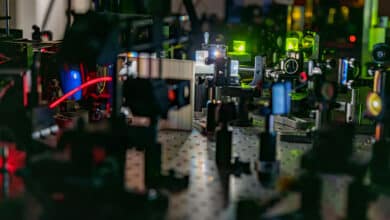
These are not incremental developments. They are signals that the photonic quantum computing modality – long dismissed by skeptics as too lossy, too probabilistic, and too far from practical computation – is entering the industrial phase. And the supply chain it draws upon looks nothing like the supply chains behind superconducting or trapped-ion quantum computers. There are no dilution refrigerators cooled to millikelvin temperatures. No chains of barium atoms suspended in electromagnetic traps. No forest of precision laser beams converging on a vacuum chamber.
Instead, there are semiconductor fabs. Photonic integrated circuits etched in silicon nitride. Superconducting nanowire detectors manufactured by the million on the same wafers as the photon sources. Barium titanate optical switches grown in the world’s largest molecular beam epitaxy tool. And telecom-standard optical fiber – the same fiber that carries your internet traffic – linking quantum processors across server racks without a single frequency transduction step.
The photonic quantum computing supply chain is, in many ways, the most radical proposition in the quantum industry: the bet that quantum computing’s hardest problem, scaling, will be solved not by exotic physics, but by industrial manufacturing. If that bet pays off, the winners won’t come from the quantum world at all. They’ll come from the semiconductor and telecommunications industries that have been building photonic infrastructure for decades.
This article maps the photonic quantum computing supply chain from foundry to photon detector, identifying the companies, bottlenecks, and strategic dynamics that will determine whether light becomes the dominant carrier of quantum information. As with our companion analyses of the superconducting and trapped-ion supply chains, the question is: if photonics wins, who else wins?
This analysis examines technology and market dynamics. It does not constitute financial or investment advice.
Anatomy of a Photonic Quantum Computer
There is no single canonical architecture for a photonic quantum computer. The field is divided along several fundamental design axes – how qubits are encoded, how gates are performed, and how errors are corrected – in ways that produce very different supply chain requirements. Understanding these distinctions is essential before mapping who provides what.
The most basic division is between discrete-variable (DV) and continuous-variable (CV) approaches. In DV systems, quantum information is encoded in discrete properties of individual photons – their polarization, path (which waveguide they travel through), or time of arrival. PsiQuantum, ORCA Computing, and Quandela use DV encodings. In CV systems, quantum information is encoded in continuous properties of light fields – the amplitude and phase quadratures of electromagnetic modes. Xanadu pioneered the CV approach, using squeezed states of light and a special type of error-protected qubit called a Gottesman-Kitaev-Preskill (GKP) state.
The second division concerns the computational model itself. PsiQuantum uses measurement-based quantum computing (MBQC) with fusion-based quantum computation: small entangled photonic “resource states” are generated and then fused together through measurements, creating a large entangled cluster state from which computation is extracted by further measurements. Xanadu’s architecture also relies on measurement-based approaches but with GKP-encoded qubits on a continuous-variable platform. Other companies, including QuiX Quantum and Quandela, pursue gate-based photonic computing, where photonic circuits implement quantum logic gates directly – more analogous to how superconducting and trapped-ion systems operate.
A third category blurs the boundary between photonic quantum computing and other modalities. Photonic Inc. (Vancouver) uses silicon T-center spin qubits – color center defects in silicon that emit photons at telecom wavelengths – to create a hybrid spin-photon platform where stationary qubits compute and photons connect them. This is not purely photonic computing, but it draws heavily on the photonic supply chain for its interconnects and integrated photonics.
Despite these architectural differences, every photonic quantum computing system requires some combination of the same physical components:
Photon sources – devices that generate single photons or squeezed light states, either through spontaneous processes in nonlinear optical materials (PsiQuantum’s approach using silicon waveguides), deterministic quantum dot emitters (Quandela, Sparrow Quantum, Aegiq), or optical parametric oscillators (Xanadu’s squeezed-light sources). Photonic integrated circuits (PICs) – chips that route, switch, and interfere photons through waveguide networks. These are fabricated in silicon, silicon nitride, or other photonic materials using semiconductor processes. Single-photon detectors – devices that register the arrival of individual photons with high efficiency and low noise. The dominant technology is the superconducting nanowire single-photon detector (SNSPD), which requires cryogenic cooling to approximately 1–4 Kelvin. Optical switches – fast, low-loss devices that route photons between different waveguide paths. These are critical for feed-forward operations and active error correction. Optical fiber – standard telecom fiber (1550 nm wavelength) for connecting photonic modules and enabling the modular, distributed architectures that give photonics its scaling thesis. Control electronics – FPGAs, DACs, and real-time processors that manage photon generation timing, switch control, detection readout, and the feed-forward logic essential for measurement-based computation. Cryogenic infrastructure – while photonic qubits themselves are generated and manipulated at or near room temperature, the SNSPD detectors that read them out require cooling to a few Kelvin. PsiQuantum operates its system at 2–4 K, warm enough to avoid the exotic cryogenics of superconducting qubits but cold enough to need helium-based cooling.
Each of these layers has its own supplier landscape, its own bottlenecks, and its own connection to the broader industrial photonics ecosystem – an ecosystem worth hundreds of billions of dollars annually. That connection is the defining feature of the photonic supply chain, and the source of both its greatest advantage and its most important strategic question: can quantum photonics actually leverage classical photonics manufacturing, or does it need something fundamentally different?
The Foundry Thesis: Why Semiconductor Manufacturing Is the Strategy
No photonic quantum computing company has articulated its supply chain strategy more explicitly than PsiQuantum. The company’s entire corporate identity is built around a single proposition: the path to a million-qubit fault-tolerant quantum computer runs through the same factories that produce chips for smartphones and automobiles.
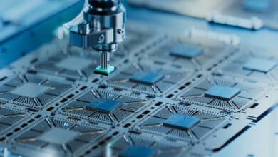
PsiQuantum’s Omega chipset – described in its February 2025 Nature paper – integrates single-photon sources, superconducting single-photon detectors, and optical switches onto a monolithic silicon photonics platform, fabricated on 300-millimeter wafers at GlobalFoundries‘ flagship Fab 8 facility in Malta, New York. The manufacturing flow involves more than twenty photolithography levels and hundreds of processing and in-line measurement steps. GlobalFoundries is now producing thousands of PsiQuantum’s wafers, using the same tools, materials, and quality control processes that it uses for its commercial semiconductor customers.
This is not a partnership of convenience. It is a strategic bet by both companies. GlobalFoundries (NASDAQ: GFS) has positioned silicon photonics as one of its core growth platforms, and quantum computing as an adjacent market. In November 2025, GlobalFoundries acquired Advanced Micro Foundry (AMF), a Singapore-based silicon photonics foundry, making it the largest pure-play silicon photonics foundry by revenue. The acquisition expands GlobalFoundries’ silicon photonics capacity across the U.S. and Asia, with the company targeting more than $1 billion in annual silicon photonics revenue by the end of the decade – driven primarily by AI data center demand for optical interconnects, but with quantum computing as a growing secondary market.
The significance of PsiQuantum’s foundry approach extends beyond manufacturing scale. By building its quantum photonic components using standard semiconductor processes and materials – silicon-on-insulator waveguides, niobium nitride superconducting films, copper interconnects – PsiQuantum inherits the semiconductor industry’s ecosystem of design tools, process control, yield management, and supply chain infrastructure. This is a fundamentally different model from the bespoke fabrication that characterizes most other quantum computing approaches, where chips are made one or a few at a time in dedicated research-grade facilities.
Xanadu pursues a related but distinct manufacturing strategy. Its photonic chips are fabricated on silicon nitride waveguides on 300-millimeter wafers – a platform shared with the rapidly growing silicon photonics industry serving classical data centers. In mid-2025, Xanadu opened a $10 million photonic packaging facility in Toronto and announced partnerships with Applied Materials for high-volume photonic chip processes and with Japan’s DISCO Corporation for ultra-low-loss wafer dicing and polishing. The March 2026 announcement of Project OPTIMISM – seeking up to CAD $390 million in government support for domestic photonic manufacturing infrastructure in Canada – signals a push toward vertical integration of photonic chip fabrication, packaging, and module assembly.
QuiX Quantum (Enschede, Netherlands), a University of Twente spin-off, also builds on silicon nitride but emphasizes a different strategic position: silicon nitride as a room-temperature, CMOS-compatible, ultra-low-loss photonic platform. QuiX has shipped over 15 photonic quantum processors worldwide and in mid-2025 secured €15 million in Series A funding to deliver what it calls the first single-photon-based universal quantum computer by 2026.
Other foundry players serve the photonic quantum ecosystem indirectly. Tower Semiconductor (NASDAQ: TSEM) is investing $650 million to triple its silicon photonics shipments by mid-2026, driven primarily by AI data center demand. IMEC (Belgium) operates one of the world’s most advanced photonic integrated circuit pilot lines and serves as a shared fabrication resource for European quantum photonics programs.
The investor read: The foundry thesis is the single most distinctive feature of the photonic quantum computing supply chain – and the most consequential for investors. If photonic quantum computers can genuinely leverage high-volume semiconductor manufacturing, the capital expenditure required to scale production falls dramatically compared to modalities that depend on bespoke fabrication. GlobalFoundries (NASDAQ: GFS) is the most direct public-market exposure to this thesis: its silicon photonics business is growing rapidly (driven by classical AI/telecom demand), and PsiQuantum’s quantum program rides on the same manufacturing platform. Tower Semiconductor (NASDAQ: TSEM) provides additional silicon photonics foundry exposure. The risk is that quantum photonic fabrication may ultimately require specialized processes and materials – barium titanate switches, superconducting detector layers, custom photon sources – that diverge from standard silicon photonics production, reducing the manufacturing leverage that justifies the photonic approach.
The Photon Source Problem: Making Light Quantum
Every photonic quantum computer begins with generating single photons or other quantum states of light. This sounds simple. It is, in fact, one of the most technically demanding challenges in the entire quantum stack.
Photon sources for quantum computing must satisfy several competing requirements simultaneously: they must produce photons that are truly single (no multi-photon contamination), highly indistinguishable from each other (essential for quantum interference), generated at precise times (on-demand rather than random), and emitted efficiently into optical waveguides or fibers. No existing photon source technology simultaneously maximizes all of these properties, and the trade-offs shape the architecture of every photonic quantum computer.
Three distinct approaches are competing.
Spontaneous parametric sources generate photon pairs through nonlinear optical processes in waveguides or crystals. When one photon of the pair is detected (“heralded”), its partner is confirmed to exist and can be used for computation. This is PsiQuantum’s approach: its Omega chipset uses resonantly enhanced spontaneous four-wave mixing in silicon waveguides to generate heralded single photons at telecom wavelength (1550 nm). The advantage is that these sources can be fabricated monolithically on the same silicon photonic chip as the rest of the quantum circuit — a massive manufacturing benefit. The disadvantage is that spontaneous sources are probabilistic: you don’t control exactly when a photon will be produced, creating a multiplexing challenge that requires fast optical switches and additional resources.
Quantum dot sources use semiconductor nanostructures – tiny islands of one material (typically indium arsenide) embedded in another (typically gallium arsenide) – that emit single photons on demand when excited by a laser pulse. Quantum dots currently produce the highest-quality single photons available: near-perfect indistinguishability, extremely low multi-photon probability, and deterministic timing. Quandela has built its entire business around quantum dot single-photon sources, commercializing a device called Prometheus – described as the world’s first standalone photonic qubit emitter. Sparrow Quantum (Copenhagen, Denmark), a spin-out from the Niels Bohr Institute, sells a competing quantum dot chip called Sparrow Core, based on indium arsenide quantum dots in photonic crystal waveguides. Aegiq (Sheffield, UK) is developing its own quantum dot platform.
The supply chain for quantum dot sources is specialized. The quantum dots are grown using molecular beam epitaxy (MBE) – a technique that deposits atomic layers of semiconductor material in ultra-high vacuum. MBE systems are expensive ($1–5 million each), and the growth of quantum-grade quantum dots requires extraordinary precision in layer thickness and composition control. The epitaxial wafers are then processed using nanofabrication techniques (electron-beam lithography, dry etching) to create micropillar cavities or photonic crystal structures that enhance the photon emission rate and collection efficiency. This is not a process that scales trivially to millions of devices.
Squeezed light sources are used in continuous-variable architectures. Xanadu generates squeezed states – quantum states of light with reduced noise in one quadrature – using optical parametric amplifiers pumped by classical laser light. These sources don’t produce single photons directly but create the non-classical light states from which GKP qubits are constructed. Xanadu’s June 2025 Nature paper on on-chip GKP state generation demonstrated this process on an integrated silicon nitride photonic chip, using photon-number-resolving detectors with over 99% efficiency.
The investor read: Photon sources are the first link in the photonic quantum chain and the most fragmented. PsiQuantum’s monolithically integrated sources on silicon represent the cleanest supply chain story – fabricated in the same foundry, on the same wafer, as everything else. Quantum dot sources (Quandela, Sparrow Quantum, Aegiq) offer superior single-photon quality but face a manufacturing scaling challenge: growing quantum dots to the specification required for quantum computing is fundamentally different from silicon semiconductor manufacturing. The question of which photon source approach prevails will determine whether the photonic quantum supply chain converges with the classical photonics industry (PsiQuantum’s thesis) or requires its own specialized component ecosystem (the quantum dot path). For the CV approach (Xanadu), the source challenge is different – squeezed light generation draws on established nonlinear optics technology – but depends on achieving extremely low optical losses that test the limits of photonic integration.
The Detector Bottleneck: Superconducting Nanowires at the Heart of Light-Based Computing
Here is the great irony of photonic quantum computing’s “room temperature” narrative: the photons travel through waveguides and fibers at room temperature, but the detectors that read them out must be superconducting.
Superconducting nanowire single-photon detectors (SNSPDs) are the gold standard for photonic quantum computing readout. A thin strip of superconducting material – typically niobium nitride (NbN), niobium titanium nitride (NbTiN), or tungsten silicide (WSi) – just a few nanometers thick and roughly 100 nanometers wide, is cooled below its superconducting critical temperature and biased with a current just below the critical current. When a single photon strikes the nanowire, it creates a localized “hotspot” that momentarily breaks the superconductivity, producing a measurable voltage pulse. The nanowire recovers in nanoseconds, ready to detect the next photon.
SNSPDs offer detection efficiencies exceeding 98% at telecom wavelengths, timing precision below 40 picoseconds, virtually zero false counts, and recovery times fast enough to count photons at rates exceeding a hundred million per second. No other detector technology comes close on the combination of these metrics.
PsiQuantum has taken the most aggressive approach to detector integration: manufacturing waveguide-integrated SNSPDs monolithically on its silicon photonic chip at GlobalFoundries. The Omega chipset incorporates niobium nitride superconducting films directly into the semiconductor manufacturing flow, producing millions of photon-number-resolving detectors on the same wafer as the photon sources and switches. This is a remarkable manufacturing achievement – integrating superconducting thin films into a CMOS-compatible process flow – and it eliminates the fiber-coupling losses that plague discrete detector systems.
For companies that don’t integrate detectors on-chip, the commercial SNSPD market provides an alternative. Key suppliers include:
ID Quantique (Geneva, Switzerland), the most established commercial SNSPD vendor, offers the ID281 system with up to 16 detectors in a single cryogenic unit, Swiss-manufactured to industrial standards. ID Quantique was acquired by IonQ in 2025 – primarily for its quantum networking capabilities, but the SNSPD technology has applications across photonic quantum computing.
Single Quantum (Delft, Netherlands) provides fiber-coupled SNSPD systems widely used in European quantum photonics laboratories and by companies such as ORCA Computing.
Pixel Photonics (Münster, Germany) has developed a distinctive approach: waveguide-integrated SNSPDs that are fabricated directly on photonic integrated circuits, serving as a subcontractor for companies like QuiX Quantum. Pixel Photonics’ waveguide-integrated design offers near-100% internal quantum efficiency with dramatically faster recovery times than conventional meandered nanowire designs.
Photon Spot (Monrovia, California) supplies free-space-coupled SNSPD systems to U.S. laboratories and quantum computing companies.
PhoTec (Shanghai, China) manufactures high-efficiency SNSPDs that have been used in China’s Jiuzhang photonic quantum computing experiments.
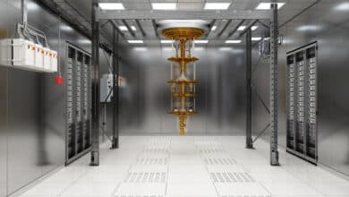
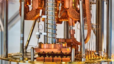
Because SNSPDs require cryogenic cooling to 1–4 Kelvin, they reintroduce a cryogenic dependency into the photonic supply chain. However, the cooling requirements are orders of magnitude less demanding than those for superconducting qubits (which operate at 10–15 millikelvin). PsiQuantum has addressed this by designing rack-based cryogenic cabinets – cooled by liquid helium in a flow similar to classical data center liquid cooling – that can accommodate hundreds of quantum chips in a single unit. These cabinets provide thousands of times the cooling power of the largest dilution refrigerator, at a fraction of the complexity and cost.
The investor read: The SNSPD supply chain is small but essential. For PsiQuantum and others pursuing on-chip detector integration, the supply chain question is primarily about superconducting materials (niobium nitride, niobium titanium nitride) and the process engineering required to deposit these films in a CMOS-compatible flow. For companies using discrete detectors, the commercial SNSPD market is served by a handful of specialized vendors – concentrated enough to be a bottleneck if demand scales rapidly, but not as concentrated as the dilution refrigerator market. The cryogenic infrastructure required for SNSPDs (closed-cycle cryocoolers operating at a few Kelvin) is mature and supplied by established players such as Cryomech (now owned by Bluefors), Sumitomo, and Oxford Instruments. This is standard cryogenics – industrial-grade, not quantum-exotic.
The Switch: Barium Titanate and the Optical Routing Challenge
If photon sources are where quantum information enters the photonic system and detectors are where it exits, optical switches are the traffic signals in between. Every measurement-based photonic quantum computer requires the ability to rapidly route photons between different waveguide paths – either to implement feed-forward logic (measuring one photon and using the result to determine the path of the next) or to dynamically reconfigure the optical circuit for different computations.
The performance requirements are severe. Switches must operate in nanoseconds (fast enough to route photons before they leave the chip), introduce minimal optical loss (every fraction of a decibel of loss destroys quantum information), and be fabricated at scale in the millions. This combination – speed, loss, and manufacturability – has been one of the hardest problems in photonic quantum computing.
PsiQuantum’s solution is barium titanate (BaTiO₃, or BTO) – a ferroelectric material with an extraordinarily strong electro-optic effect. BTO switches can change state in nanoseconds with applied voltages of just a few volts, achieving switching speeds and extinction ratios that no silicon-based thermal or carrier-injection switch can match. PsiQuantum built what it describes as the world’s largest molecular beam epitaxy tool specifically to grow BTO thin films on silicon wafers at the quality and volume required for quantum computing. The BTO switches are then bonded to the silicon photonic wafers in a separate processing step – part of the Omega chipset’s multi-level fabrication flow.
This is a strategic supply chain choice. Barium titanate is not a standard semiconductor material. It doesn’t appear in GlobalFoundries’ normal process offerings. PsiQuantum had to develop the growth process, the wafer bonding process, and the device fabrication process from scratch. The company’s partnership with NY CREATES (the R&D center at the Albany NanoTech Complex) specifically targets integrating BTO switches with the silicon photonic platform.
Other approaches to optical switching exist in the photonic quantum ecosystem. Xanadu and QuiX Quantum primarily use thermo-optic switches (where heating a waveguide changes its refractive index), which are simpler to fabricate but much slower (microsecond scale rather than nanosecond) and consume more power. For their architectures, this may be acceptable – Xanadu’s continuous-variable approach and QuiX’s gate-based approach have different timing requirements than PsiQuantum’s fusion-based measurement scheme. ORCA Computing uses a combination of fiber-based time-domain multiplexing and spatial routing via optical switches.
The broader photonics industry is also investing heavily in electro-optic switching for classical applications. The explosion of AI training workloads has created massive demand for faster optical interconnects in data centers, and several companies – including Lightmatter, Ayar Labs, and Coherent – are developing high-speed optical switches for co-packaged optics. BTO and lithium niobate (LiNbO₃) are both emerging as materials for next-generation electro-optic modulators in the classical telecom space, creating a potential overlap where quantum and classical photonics share process development costs.
The investor read: Optical switching is a cross-cutting bottleneck that affects photonic quantum computing differently depending on the architecture. PsiQuantum’s bet on barium titanate is high-risk, high-reward: BTO delivers superior performance but requires a novel materials supply chain that doesn’t exist at industrial scale. If BTO switches prove essential for fault-tolerant photonic quantum computing, PsiQuantum’s early investment in BTO manufacturing infrastructure becomes a significant moat. The classical AI/telecom demand for faster electro-optic switches could accelerate BTO process development, creating a dual-use market that benefits quantum photonics. For investors, the broader photonic switching market – driven by AI data center buildout – is orders of magnitude larger than the quantum computing application and will determine whether BTO and similar materials reach the manufacturing maturity that quantum photonics requires.
Photonic Integrated Circuits: The Processing Layer
The heart of a photonic quantum computer is the photonic integrated circuit – a chip containing waveguides that guide, split, interfere, and route single photons. The PIC performs the quantum operations: beam splitters implement quantum gates, phase shifters adjust qubit states, and interferometric networks create the entanglement and interference patterns that enable quantum computation.
Three waveguide material platforms dominate photonic quantum computing:
Silicon-on-insulator (SOI) is PsiQuantum’s primary waveguide platform, chosen for its direct compatibility with standard CMOS fabrication at GlobalFoundries. Silicon waveguides at telecom wavelengths are highly compact (enabling high integration density) and benefit from the massive infrastructure investment of the classical silicon photonics industry. The trade-off is that silicon has higher propagation loss than silicon nitride, and its smaller waveguide mode volume makes it more sensitive to fabrication imperfections.
Silicon nitride (Si₃N₄) is the platform of choice for Xanadu, QuiX Quantum, and several other photonic quantum companies. Silicon nitride offers dramatically lower optical propagation loss than silicon – a critical advantage for quantum applications where every fraction of a decibel matters. It’s also transparent across a wider wavelength range (from visible to mid-infrared), which enables some photon source technologies that silicon cannot support. The fabrication process is CMOS-compatible, and silicon nitride PICs can be manufactured on 200mm or 300mm wafers at commercial foundries including IMEC, LioniX International (Enschede, Netherlands), and others.
Indium phosphide (InP) and lithium niobate (LiNbO₃) play supporting roles. InP is essential for active photonic components – lasers, amplifiers, and high-speed modulators – that silicon cannot efficiently produce. Thin-film lithium niobate on insulator (LNOI) offers the strongest electro-optic effect of any widely available material and is used for fast modulators and switches. Both platforms are served by established specialty foundries, though neither has the manufacturing scale of silicon photonics.
The companies that fabricate photonic integrated circuits for quantum applications are a mix of integrated quantum companies and specialized photonic foundry services:
LioniX International (Netherlands) operates the TriPleX platform – a multi-layer silicon nitride waveguide technology that is used by QuiX Quantum and other photonic quantum computing companies. LioniX’s technology enables extremely low-loss waveguides and complex interferometric networks.
IMEC (Belgium) offers pilot-line access for photonic integrated circuit fabrication, including processes for both silicon and silicon nitride photonics. IMEC’s role in the European quantum ecosystem is analogous to its role in the classical semiconductor ecosystem: a shared R&D and fabrication resource that multiple companies can access without building their own fabs.
Ligentec (Geneva, Switzerland) is a silicon nitride PIC foundry that serves quantum photonics customers alongside classical photonics applications.
The photonic packaging challenge deserves specific mention. Connecting photonic chips to optical fibers, detectors, and control electronics with minimal loss is a deceptively difficult engineering problem. Xanadu’s new packaging facility in Toronto and its partnerships with Applied Materials and DISCO specifically target this bottleneck. The QUPICS program – a U.S. Department of Defense initiative involving TOPTICA, BluGlass, and others – aims to develop 300mm foundry-scale fabrication for quantum photonic integrated circuits spanning ultraviolet through infrared.
The investor read: Photonic integrated circuits represent the layer where the “semiconductor supply chain” thesis for quantum photonics is most credible. The waveguide fabrication processes are genuinely compatible with existing foundry infrastructure, and the same platforms (silicon, silicon nitride) serve both quantum and classical photonics markets. The classical silicon photonics market is projected to exceed $1 billion annually by decade’s end (GlobalFoundries alone is targeting this figure), providing scale economies that quantum photonics can ride. For investors, the PIC layer is less a collection of investable quantum-specific companies and more a beneficiary map of existing photonic foundries and packaging companies whose quantum revenue will grow as photonic quantum computers scale. GlobalFoundries (GFS), Tower Semiconductor (TSEM), and the broader silicon photonics supply chain all sit at this intersection.
The Big Players: Five Architectures, Five Supply Chains
The photonic quantum computing market is more architecturally diverse than either the superconducting or trapped-ion markets. Five companies represent five distinct approaches to photonic quantum computing, each with different supply chain dependencies.
PsiQuantum: The Factory-First Approach
PsiQuantum (Palo Alto, California) is the most heavily capitalized photonic quantum computing company, having raised approximately $1.7 billion. Its thesis is that only manufacturing-first, fault-tolerant-first design can deliver useful quantum computing. PsiQuantum’s Alpha System – a prototype being assembled at a facility in Milpitas, California – is designed to validate the full Omega chipset architecture. The system was expected to begin cryogenic operation by late 2025, with experiments beginning in early 2026. Sites for utility-scale systems are under development in Brisbane (backed by the Australian government) and Chicago.
PsiQuantum’s supply chain is uniquely concentrated: GlobalFoundries for chip fabrication, in-house BTO growth in San Jose, and a modular cryogenic rack architecture that eschews dilution refrigerators in favor of liquid-helium-cooled cabinets. The company’s leadership transition in February 2026 – with Victor Peng (former president of AMD and CEO of Xilinx) becoming interim CEO – signals a shift from R&D to execution and deployment.
Xanadu: The Modular Photonic Data Center
Xanadu (Toronto, Canada) pioneered the continuous-variable approach and is building toward what it calls a “quantum data center” by 2029. Aurora, its 12-qubit prototype, demonstrated modular networked quantum computing across four interconnected server racks, 35 photonic chips, and 13 kilometers of optical fiber – all operating at room temperature. Xanadu’s GKP qubit approach, validated through publications in Nature and Physical Review Letters, provides an intrinsic layer of error protection that may reduce the total qubit overhead for fault tolerance.
Xanadu’s SPAC merger with Crane Harbor Acquisition Corp., valued at $3.1 billion, is expected to make it the first publicly traded pure-play photonic quantum computing company, with shares on both Nasdaq and TSX under the ticker XNDU. The company’s software platform – PennyLane, an open-source quantum machine learning framework – is widely used across the quantum community regardless of hardware modality, providing a software revenue base.
Quandela: The Quantum Dot Full-Stack
Quandela (Massy, France) is the leading European photonic quantum computing company and the only one built around deterministic quantum dot single-photon sources. Its current system, Belenos, delivers 12 qubits and is deployed commercially in France and beyond. The company’s open-source SDK, Perceval, has 1,200+ users across 30 countries. Quandela’s November 2025 MoU with the Seoul Metropolitan Government, worth up to approximately $57 million, aims to establish an R&D and manufacturing hub in Korea – strategically positioning European photonic quantum IP alongside Korean semiconductor manufacturing expertise.
Quandela claims its hybrid architecture reduces the number of fault-tolerant components by a factor of 100,000 compared to purely photonic competitors – a theoretical result awaiting hardware validation but with significant intellectual property implications.
ORCA Computing: The Defense-Engaged Compact System
ORCA Computing (London, UK) builds compact, rack-mounted photonic quantum computers using time-bin-encoded single photons stored in quantum memories based on rubidium atomic ensembles. ORCA’s PT Series systems use telecom-standard components and can be deployed in standard server rack environments. The company has secured significant UK Ministry of Defence contracts, deployed nine commercial PT-1 systems globally, and is targeting its PT-3 system in 2026 to demonstrate computational advantages over GPU clusters for quantum machine learning workloads.
ORCA’s supply chain draws on photonic components from Sparrow Quantum (quantum dot sources), Pixel Photonics (waveguide-integrated SNSPDs), and its own in-house integrated photonics division acquired from GXC in Texas.
QuiX Quantum: The European Room-Temperature Processor
QuiX Quantum (Enschede, Netherlands) positions itself as Europe’s leading photonic quantum computing hardware supplier. Its photonic processors, built on LioniX International‘s TriPleX silicon nitride platform, have been sold to the German Aerospace Center (DLR) and deployed across European research institutions. QuiX’s $17 million Series A in 2025 funds development of a universal photonic quantum computer by 2026, with error-correcting systems targeting 2027.
The investor read: PsiQuantum and Xanadu are the two highest-conviction bets on photonic quantum computing. PsiQuantum is private, reportedly considering a public listing, and represents the purest “semiconductor supply chain” investment thesis. Xanadu’s pending Nasdaq listing (ticker XNDU) would provide the first direct public equity in photonic quantum computing. Quandela and ORCA offer European exposure with defense and sovereignty angles. QuiX is earlier-stage but represents the open-hardware photonic processor market. Unlike the superconducting market (where IBM and Google dominate as vertically integrated giants), the photonic market has no incumbent behemoth — every player is a startup, and the ecosystem is still forming. This creates both opportunity and risk: there is no “safe” choice, but the total addressable market is potentially larger because photonic quantum computers may be cheaper and easier to deploy than cryogenically intensive alternatives.
The Telecom Inheritance: Why Fiber Optics Matters
One of the most strategically significant features of photonic quantum computing is that many of its architectures use telecom-wavelength photons (1550 nm) that travel natively over standard optical fiber. This means that photonic quantum modules can be connected using the same fiber infrastructure that underpins the global internet – without the frequency transduction steps that other modalities require to convert their qubit signals into optical signals for networking.
PsiQuantum explicitly builds on this. Its Omega chipset generates, processes, and detects photons at 1550 nm. Modules are connected by standard optical fiber. Xanadu’s Aurora demonstrated inter-rack quantum operation over 13 kilometers of fiber. Photonic Inc. – whose silicon T-center qubits emit at telecom wavelengths – has raised this to a central architectural thesis, arguing that its distributed quantum computing platform can scale out across data centers and even between cities using existing telecom infrastructure.
The supply chain implications are profound. The global optical fiber market, dominated by companies like Corning (NYSE: GLW), Prysmian, and Furukawa Electric, produces hundreds of millions of kilometers of fiber annually. Optical connectors, splitters, and passive components from Thorlabs, OZ Optics, and others are commodity items. This is not a supply chain that will be strained by quantum computing demand.
What this means for scaling is that photonic quantum computing has a modularity advantage built into its physics. Where superconducting quantum computers must scale primarily within a single cryostat (creating the cabling and cooling bottleneck described in our superconducting analysis), and trapped-ion systems face the unproven challenge of photonic interconnects between modules, photonic quantum computers can in principle scale out by simply adding more racks connected by more fiber. Whether this works in practice – whether the entanglement rates achievable over fiber are fast enough for useful fault-tolerant computation – remains the central engineering question.
The investor read: The telecom fiber inheritance is photonic quantum computing’s strongest supply chain advantage. It means that scaling doesn’t require a new physical infrastructure – it leverages an existing one. For investors, this reduces the capital intensity of deployment and opens the possibility that quantum computing infrastructure might eventually integrate into existing data center fiber plants. Companies like Corning and the fiber optic supply chain are potential indirect beneficiaries, though quantum computing represents a tiny fraction of overall fiber demand. The deeper strategic implication is for data center operators: photonic quantum computing is architecturally the most compatible modality with existing classical data center infrastructure, which could accelerate enterprise adoption.
The Geopolitics of Photons: Sovereignty, Manufacturing, and the AI-Quantum Nexus
The photonic quantum computing supply chain intersects with one of the most intense geopolitical competitions of the 2020s: the race for semiconductor manufacturing supremacy. Because photonic quantum computers are manufactured in semiconductor fabs, the same policy dynamics that shape the CHIPS Act, European Chips Act, and China’s semiconductor self-sufficiency programs directly affect the quantum photonics supply chain.
PsiQuantum’s relationship with GlobalFoundries – a U.S.-headquartered company with fabs in New York, Vermont, Germany, and Singapore – places its manufacturing within the sphere of U.S. and allied semiconductor policy. The Australian government’s backing of PsiQuantum’s Brisbane site reflects a sovereign quantum strategy built around photonic manufacturing. Xanadu’s Project OPTIMISM in Canada aims to establish domestic heterogeneous integration, photonic packaging, and quantum module assembly capabilities – explicitly framed as a sovereignty play.
In Europe, the photonic quantum ecosystem benefits from the same industrial policy support that flows into the broader European photonics industry. The Netherlands, home to QuiX Quantum, PhotonDelta (a public-private partnership supporting the Dutch photonic ecosystem), and ASML (whose lithography machines make all of this possible), has a uniquely strong position. France’s Quandela benefits from the French national quantum strategy and research infrastructure. Germany’s PhotonicsForQT initiative supports the broader intersection of photonics and quantum technology.
China has invested heavily in photonic quantum computing. The Jiuzhang experiments at the University of Science and Technology of China (USTC) demonstrated quantum advantage in Gaussian boson sampling with up to 255 detected photons. QBoson recently broke ground on the world’s first dedicated photonic quantum computer manufacturing facility in Shenzhen, expected to produce dozens of units annually. China’s photonic quantum effort draws on its domestic SNSPD manufacturing capabilities (PhoTec and others) and its substantial classical photonics industry.
The AI-quantum nexus adds another dimension. The same silicon photonics infrastructure that PsiQuantum uses for quantum computing is being scaled up massively to serve AI data center demand for optical interconnects. NVIDIA’s Quantum-X and Spectrum-X photonic switches, built with TSMC and partners, are driving silicon photonics foundry demand to unprecedented levels. This creates a competitive tension: as AI demand absorbs silicon photonics fab capacity, quantum photonics programs may face allocation conflicts at shared foundries. It also creates an opportunity: the process development, equipment investment, and yield engineering driven by AI-scale photonics demand benefits quantum photonics as a free rider.
The investor read: Photonic quantum computing is uniquely positioned at the intersection of quantum technology policy and semiconductor industrial policy. Unlike superconducting (which depends on a specialized cryogenics supply chain disconnected from broader industrial policy) or trapped ions (which depend on precision laser and vacuum technology), photonic quantum computing rides the semiconductor and telecom policy waves directly. Government investments in photonic manufacturing – whether motivated by AI, telecom, or quantum – all benefit the photonic quantum supply chain. The risk is also clear: if the AI photonics buildout absorbs all available fab capacity, quantum programs could be deprioritized by foundries serving much larger commercial customers.
Who Wins If Photonics Wins: An Ecosystem Map
Tier 1: Direct, High-Concentration Beneficiaries
GlobalFoundries (NASDAQ: GFS) – The foundry partner for PsiQuantum and the largest pure-play silicon photonics foundry. If photonic quantum computers are manufactured at scale, GlobalFoundries’ Fab 8 is where many of them will be made. The company’s silicon photonics business is growing independently through AI/telecom demand, providing a revenue base that sustains quantum-relevant process development.
PsiQuantum (private, reportedly considering public listing) – The most heavily capitalized photonic quantum company, with the most direct foundry-manufacturing thesis. If photonics wins and the factory-first approach works, PsiQuantum’s Omega chipset and utility-scale deployment model position it as a potential platform leader.
Xanadu (pending Nasdaq listing as XNDU) – The first pure-play photonic quantum computing public stock, with a modular room-temperature architecture, the widely adopted PennyLane software platform, and growing government backing. Xanadu’s GKP-based continuous-variable approach offers a differentiated path to fault tolerance.
Quandela (private, France) – Europe’s leading photonic quantum computing company and the global leader in quantum dot single-photon sources. Quandela’s Seoul MoU and French government backing provide a dual-continent manufacturing and commercialization strategy.
Tier 2: Enabling Technology Providers
Single-photon detector suppliers – ID Quantique (Switzerland, owned by IonQ), Single Quantum (Netherlands), Pixel Photonics (Germany), Photon Spot (U.S.) – companies whose SNSPD technology is essential for nearly all photonic quantum computing architectures.
Photonic foundries and PIC suppliers – LioniX International (Netherlands), IMEC (Belgium), Ligentec (Switzerland), Tower Semiconductor (NASDAQ: TSEM) – specialized foundries that fabricate photonic integrated circuits for quantum and classical applications.
Sparrow Quantum (private, Denmark) and Aegiq (private, UK) – Quantum dot single-photon source specialists supplying components to multiple photonic quantum computing companies.
Photonics component suppliers – Thorlabs, Coherent (NYSE: COHR), Gooch & Housego – broad-market photonics companies whose components (modulators, fibers, lenses, optical assemblies) appear throughout photonic quantum systems.
Tier 3: Software, Integration, and Emerging Plays
ORCA Computing (private, UK) – Compact room-temperature photonic systems with UK defence contracts. Differentiated by quantum memory architecture and near-term hybrid quantum-classical positioning.
QuiX Quantum (private, Netherlands) – European photonic quantum processor supplier, positioned as the “QuantWare of photonics” – an open-hardware component vendor rather than a full-stack system maker.
Photonic Inc. (private, Canada) – The T-center spin-photon hybrid approach, backed by Microsoft, with $271 million raised. Not purely photonic but deeply dependent on the photonic supply chain for its telecom-fiber-based distributed architecture.
Riverlane (private, UK) – Quantum error correction technology applicable across modalities, including photonic systems approaching fault tolerance.
Q-CTRL (private, Australia) – Hardware-agnostic quantum control optimization software used by companies across the photonic ecosystem.
Tier 4: Infrastructure and Cross-Market Beneficiaries
Corning (NYSE: GLW) and optical fiber suppliers – Indirect beneficiaries as photonic quantum computers scale out through fiber-connected modules.
Cryocooler manufacturers – Cryomech (now owned by Bluefors), Sumitomo, Oxford Instruments – suppliers of the 4K-class cryogenic systems needed for SNSPD operation.
NVIDIA (NASDAQ: NVDA) – Through its NVentures investment in PsiQuantum and collaboration on GPU-QPU integration, and its own silicon photonics switching platforms for AI, NVIDIA sits at the nexus of AI and photonic quantum computing.
Cloud providers – AWS, Azure, and Google Cloud serve as distribution channels for photonic quantum computing access. Xanadu (AWS Braket), ORCA (various), and QuiX (cloud service) all provide cloud-based access.
Photonic vs. Superconducting vs. Trapped Ions: A Supply Chain Comparison
For investors and executives evaluating across quantum modalities, the supply chain differences are as strategically significant as the physics:
Manufacturing paradigm. Superconducting chips use specialized Josephson junction fabrication incompatible with standard CMOS. Trapped-ion chips are fabricated at semiconductor foundries (primarily Infineon). Photonic chips are fabricated at silicon photonics foundries (GlobalFoundries, Tower) – the closest to mainstream semiconductor manufacturing of any modality.
Cryogenic requirements. Superconducting: 10–15 millikelvin (dilution refrigerators, helium-3). Trapped ions: room temperature to 15 Kelvin. Photonic: room temperature for qubits, 1–4 Kelvin for detectors. The photonic cryogenic burden is real but manageable with standard industrial cryogenics.
Materials risk. Superconducting depends on niobium (90% from Brazil), helium-3, and ultra-pure aluminum. Trapped ions use commodity materials. Photonic uses standard silicon, silicon nitride, and telecom-grade optical fiber – with the exception of barium titanate (PsiQuantum) and niobium nitride (for SNSPDs), which are specialized but not geopolitically constrained.
Scaling architecture. Superconducting scales within a single cryostat (wiring and cooling bottleneck). Trapped ions pursue modular scaling via photonic interconnects or ion transport (unproven). Photonic scales natively through fiber-connected modules – architecturally the simplest path to modularity, but dependent on achieving sufficient entanglement rates between modules.
Gate speed and fidelity. Superconducting gates: nanoseconds, fidelity ~99.5–99.9%. Trapped ions: milliseconds, fidelity ~99.9–99.99%. Photonic gates: picoseconds to nanoseconds, but probabilistic (requiring post-selection), which affects effective fidelity and overhead. The probabilistic nature of photonic gates is the fundamental physics challenge that PsiQuantum’s fusion-based architecture and Xanadu’s GKP approach attempt to address through clever encoding and error correction.
What Could Derail the Photonic Supply Chain
Loss hasn’t been conquered. Optical loss – photons being absorbed or scattered before they can be measured – remains the existential challenge for photonic quantum computing. Every dB of loss reduces the probability of successful quantum operations, requiring exponentially more resources for error correction. PsiQuantum’s Nature paper demonstrated impressive component-level fidelities (99.98% state preparation, 99.22% fusion fidelity), but these numbers are conditional on photon detection and don’t account for loss. Whether the total system loss budget can be managed at the scale of millions of components is an open question.
The deterministic gate problem. Photonic two-qubit gates are inherently probabilistic – they succeed only a fraction of the time. This is not a fabrication issue; it’s a fundamental property of linear optics. PsiQuantum, Xanadu, and others have theoretical frameworks (fusion-based computing, GKP encoding) that work around this limitation through redundancy and error correction, but the resource overhead is substantial. If these overhead costs prove higher than projected, photonic quantum computers may need dramatically more physical qubits – and more manufacturing capacity – than current roadmaps assume.
Foundry competition with AI. The AI-driven demand for silicon photonics manufacturing is a double-edged sword. In the near term, it drives investment in the processes and infrastructure that quantum photonics needs. In the medium term, it could mean that GlobalFoundries, Tower, and other foundries prioritize their highest-revenue customers (hyperscaler AI companies) over their quantum programs if capacity becomes constrained. PsiQuantum’s status as a major customer at GlobalFoundries provides some protection, but the competitive dynamics bear watching.
Neutral-atom overlap. Neutral-atom quantum computing (pursued by QuEra, PASQAL, and others) shares certain supply chain elements with photonic quantum computing – particularly in the area of high-power laser systems and precision optics. More fundamentally, neutral atoms have recently demonstrated rapid scaling (QuEra’s 256-qubit system on AWS Braket) and are pursuing error-corrected computation on a timeline competitive with photonic approaches. If neutral atoms achieve fault tolerance first, the photonic-specific supply chain (SNSPDs, photon sources, BTO switches) faces stranded-asset risk.
No demonstrated quantum advantage. As of early 2026, no photonic quantum computer has demonstrated a useful computation that a classical computer cannot perform. China’s Jiuzhang experiments showed quantum advantage in Gaussian boson sampling – a specific task with limited practical applications. The gap between boson sampling demonstrations and fault-tolerant, useful quantum computation remains very large. PsiQuantum’s decision to skip NISQ-era demonstrations and build directly for fault tolerance is a calculated bet that intermediate milestones are distractions — but it also means the company has no public proof points for its architecture beyond component-level results.
Actionable Takeaways
For investors evaluating the photonic quantum ecosystem: photonic quantum computing offers the widest range of public-market entry points among the emerging modalities. GlobalFoundries (NASDAQ: GFS) provides foundry-level exposure to the manufacturing thesis. Xanadu’s pending Nasdaq listing (ticker XNDU) would provide the first direct photonic quantum equity. Coherent (NYSE: COHR) and Tower Semiconductor (NASDAQ: TSEM) offer broader photonics exposure with quantum upside. The most differentiated investment thesis in photonic quantum computing is the manufacturing one: if photonic quantum systems can genuinely leverage semiconductor fab infrastructure, the capital cost to scale drops below that of any competing modality. Assess whether your quantum portfolio is concentrated in superconducting or trapped-ion plays; the photonic supply chain is different enough that cross-modality diversification provides genuine risk reduction.
For technology executives evaluating quantum partnerships: photonic quantum computers’ room-temperature operation (at the qubit level), compact form factors (Xanadu’s server racks, ORCA’s PT Series), and fiber-based connectivity make them potentially the most data-center-compatible quantum computing modality. The key questions for a photonic quantum partner: what is their loss budget at scale, and has it been validated in an integrated system? Can their architecture perform fault-tolerant computation, or only boson sampling? And are they dependent on a single foundry – creating the same concentration risk that the superconducting ecosystem faces with cryogenics?
For policymakers shaping quantum strategy: photonic quantum computing uniquely leverages existing semiconductor industrial policy. Investments in silicon photonics manufacturing – motivated by AI, telecom, or quantum – all benefit the photonic quantum supply chain. The EU’s strong position in photonics components (IMEC, LioniX, Ligentec), the Netherlands’ photonic ecosystem (QuiX Quantum, PhotonDelta), and France’s quantum dot technology (Quandela, CNRS) give Europe genuine advantages in the photonic modality. The sovereignty risk is at the foundry level: if photonic quantum chip fabrication remains concentrated at GlobalFoundries in the U.S. and a handful of European and Asian foundries, nations without domestic silicon photonics capacity will depend on foreign manufacturing for their quantum programs.
The Light at the End of the Supply Chain
The photonic quantum computer doesn’t look like a chandelier or an optical table. In PsiQuantum’s vision, it looks like a data center: rows of liquid-cooled cabinets, each containing hundreds of silicon photonic chips, connected by the same fiber optic cables that carry the world’s internet traffic. In Xanadu’s vision, it’s a room of server racks, modular and networkable, expanding as compute demands grow. In Quandela’s vision, it’s a room-temperature system built around semiconductor quantum dots, deployable in a standard 19-inch rack.
The supply chain behind these visions draws from the deepest wells of industrial capability that civilization has built: semiconductor manufacturing, telecommunications infrastructure, and precision photonics. That is the photonic modality’s fundamental bet – that quantum computing’s scaling challenge is better solved by the world’s most mature manufacturing ecosystem than by the world’s most advanced cryogenic systems or the world’s most precise laser laboratories.
Whether the bet pays off depends on physics that remains unproven at scale: whether optical loss can be tamed across millions of components, whether probabilistic photonic gates can be made fault-tolerant through encoding and redundancy, and whether the systems-level integration of sources, circuits, switches, and detectors can be achieved within the manufacturing tolerances of commercial semiconductor fabs.
The companies that answer these questions will determine whether light becomes not just the carrier of quantum information, but the medium through which quantum computing finally arrives at industrial scale. And if it does, the supply chain winners won’t look like quantum companies at all. They’ll look like the semiconductor foundries, telecom infrastructure builders, and photonics manufacturers that already power the classical world – with a quantum dividend they didn’t know they were earning.
This article is part of PostQuantum.com’s Quantum Ecosystem series, mapping the technologies, companies, and supply chains that make quantum computing possible. For the parallel analyses of the superconducting and trapped-ion modalities, see The Chandelier’s Hidden Supply Chain and The Optical Table’s Hidden Supply Chain. For more on quantum computing modalities, see our Taxonomy of Quantum Computing Modalities.
Quantum Upside & Quantum Risk - Handled
My company - Applied Quantum - helps governments, enterprises, and investors prepare for both the upside and the risk of quantum technologies. We deliver concise board and investor briefings; demystify quantum computing, sensing, and communications; craft national and corporate strategies to capture advantage; and turn plans into delivery. We help you mitigate the quantum risk by executing crypto‑inventory, crypto‑agility implementation, PQC migration, and broader defenses against the quantum threat. We run vendor due diligence, proof‑of‑value pilots, standards and policy alignment, workforce training, and procurement support, then oversee implementation across your organization. Contact me if you want help.
Related Content