Table of Contents
(This profile is one entry in my 2025 series on quantum hardware roadmaps and CRQC risk. For the cross‑vendor overview, filters, and links to all companies, see Quantum Hardware Companies and Roadmaps Comparison 2025.)
Introduction
Photonic Inc. is a Vancouver-based quantum computing startup pioneering a distributed, fault-tolerant quantum computer architecture built on silicon spin qubits that are optically linked by photons. In contrast to monolithic quantum processors, Photonic’s design treats networking as a native feature: qubit modules are entangled together via telecom-fiber links, effectively combining quantum computing and quantum communication into one platform. The company’s approach centers on a particular spin qubit in silicon known as the “T centre” defect, which provides a missing photonic interface to silicon qubits – enabling them to emit and receive photons at telecom wavelengths for entanglement. Photonic’s founders argue this technology unlocks the first credible path toward truly scalable and useful quantum computing in silicon, overcoming the scaling roadblocks of earlier architectures.
Founded by Dr. Stephanie Simmons (a leading silicon quantum researcher at Simon Fraser University) and led by CEO Dr. Paul Terry, Photonic has quickly garnered significant support. By late 2023 the company raised $140 million USD in funding from major investors – including Microsoft and the British Columbia Investment Management Corp – to accelerate its ambitious roadmap. Microsoft in particular became both an investor and partner, aligning Photonic’s hardware with Azure’s quantum ecosystem.
Photonic has also drawn interest from defense programs: in November 2025, it was one of 11 companies selected by DARPA’s Quantum Benchmarking Initiative (QBI) to advance to Stage B after successfully proposing a “utility-scale” quantum computer concept in Stage A. This validates that external experts see Photonic’s unique architecture – based on optically-linked silicon spin qubits – as a plausible route to a large-scale quantum computer. Notably, QBI’s goal is to verify if any approach (such as Photonic’s) can achieve an industrially useful, fault-tolerant quantum computer by 2033.
Photonic, however, aims to beat that timeline: the company boldly stated it could deliver a scalable, distributed fault-tolerant quantum computing solution within five years (by ~2028), significantly sooner than the conventional forecasts. This aggressive timeline, if met, would have far-reaching implications for quantum computing and cybersecurity.
Milestones & Roadmap
Photonic’s development path so far has been marked by rapid technical progress on its silicon-photonic quantum platform. Key milestones in its roadmap include:
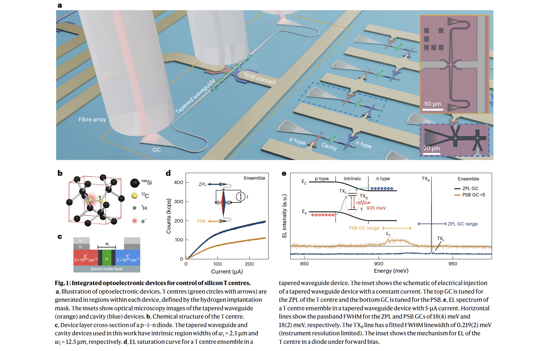
- 2020 – First T-Center Qubit Identified: Academic researchers (including Photonic’s founders) demonstrated the first isolated T-centre spin defect in silicon as a quantum bit, showing it could be optically observed and have long-lived spin states. This defect consists of two carbon atoms and one hydrogen in silicon, and crucially emits single photons at ~1326 nm (telecom O-band)– a wavelength ideal for low-loss fiber transmission.
- 2022 – Photonic Integration Achieved: The team integrated T-centres into nanofabricated silicon photonic structures on-chip. They built devices where single T-centre qubits were coupled to waveguides and optical cavities, demonstrating on-chip generation and routing of telecom single photons. This was a pivotal step showing that CMOS-compatible processes can embed quantum light sources in silicon, marrying quantum bits with semiconductor photonics.
- 2023 – Architecture Unveiled & Funding: Photonic emerged from stealth in late 2023, announcing its “Entanglement First™” architecture for a networked quantum computer and raising a $100 M round (total $140 M) to fuel development. The company revealed its plan to build “one of the world’s first scalable, fault-tolerant, and unified quantum computing and networking platforms” based on photonically linked silicon spin qubits. Dr. Simmons declared that within five years Photonic expects to offer a distributed, fault-tolerant quantum solution, arguing the silicon T-centre provides the breakthrough needed to dramatically accelerate quantum timelines. In November 2023, Photonic also formed a strategic collaboration with Microsoft to co-innovate on quantum networking and integrate Photonic’s hardware into the Azure cloud as it matures. This partnership underscored the industry’s confidence in Photonic’s roadmap.
- May 2024 – Distributed Entanglement Demonstrated: Photonic announced a significant experimental milestone: it succeeded in optically entangling qubits located in separate quantum modules (separate cryostats), performing a “teleported CNOT” gate between two remote silicon spin qubits connected by telecom fiber. While many quantum architectures only entangle qubits on the same chip, this was one of the first demonstrations of entanglement between chips in a silicon-based system. In other words, Photonic literally went “outside the box” – linking two quantum processors with photonic signals. Achieving this distributed entanglement is a proof-of-concept for Photonic’s modular scaling approach, tackling the “scaling beyond a single node” challenge in quantum computing. Microsoft’s quantum engineering team acknowledged this as a fundamental capability on the path to networked quantum computing. An especially notable result was that Photonic executed a remote two-qubit gate with these entangled modules (a teleportation-based CNOT), confirming that quantum logic operations can be performed over distance in their system. This set a new bar for the industry’s roadmaps – highlighting that modular, networked quantum computing isn’t just theory but is being realized in practice.
- Feb 2025 – Error-Correction Breakthrough (QLDPC Codes): Emphasizing its focus on fault tolerance, Photonic unveiled a new family of Quantum Low-Density Parity Check (QLDPC) codes (nicknamed “SHYPS” codes) that it developed to dramatically reduce error-correction overheads. In a news release and accompanying paper, Photonic showed that these QLDPC codes can perform arbitrary quantum logic while using up to 20× fewer physical qubits compared to traditional surface codes. This is an “industry first” solution to a decades-long challenge – enabling error-corrected quantum computing with far less resource overhead. As Dr. Simmons noted, unlocking high-performance QLDPC codes had been a “holy grail” for quantum error correction; Photonic announced it has effectively “cracked these codes”, moving the goalposts for useful quantum computing 20× closer. Notably, such codes require extremely high qubit connectivity to implement, which plays to Photonic’s architectural strengths (their entanglement-first design provides the needed connectivity within and between modules). This advance in error correction research, validated through extensive simulations, could accelerate Photonic’s roadmap by slashing the number of qubits required for fault-tolerant computing.
- Sep 2025 – Electrically Triggered Spin-Photon Device in Silicon (Nature Photonics): SFU and Photonic Inc. reported the first electrically injected single-photon source in silicon using T-centre defects, integrated in nanophotonic p-i-n diode structures. The work also demonstrated heralded spin initialization (~92% fidelity) via detected telecom-band photons, showing that T-centre spin qubits can be driven and prepared using standard electronic pulses (not only lasers). This materially advances CMOS-compatible, parallelizable qubit control and on-chip light sources for scalable, fiber-ready quantum processors.
- Late 2025 – DARPA QBI Stage B and Beyond: In November 2025, Photonic was advanced to Stage B of DARPA’s Quantum Benchmarking Initiative, having passed the Stage A concept review with its utility-scale quantum computer design. In Stage A, Photonic presented a detailed blueprint for a “Utility-Scale Quantum Computer” (USQC) based on its optically-linked silicon spin qubits, which DARPA found sufficiently plausible. Stage B (a one-year phase) will rigorously scrutinize Photonic’s R&D roadmap and risk mitigation plans to assess whether their proposed path to building this machine is truly feasible. Success in Stage B could unlock additional DARPA funding and lead into Stage C, where actual prototype construction and testing would occur under independent validation. The QBI program’s end goal is a full-scale, economically useful quantum computer by 2033. Photonic’s own targets are arguably more aggressive – aiming to demonstrate a scalable, fault-tolerant quantum system before 2030 – but participating in QBI provides external benchmarks and could de-risk the journey. By late 2025, Photonic had also grown to over 150 employees across Canada, the US, and UK, and had announced plans to open a new quantum R&D facility in the UK. The next milestones on Photonic’s roadmap will likely include scaling up the number of interconnected qubits per module, increasing the entanglement rates between modules, and implementing logical qubits using their QLDPC codes. If they continue to hit their milestones, Photonic aims to be among the first to offer cloud-accessible, error-corrected quantum computing services – potentially heralding a major step toward the reality of utility-scale quantum computing well ahead of schedule.
Focus on Fault Tolerance
From the outset, Photonic’s architecture has been explicitly designed with fault tolerance in mind. The company’s philosophy is that scaling to useful quantum computers demands early integration of error correction and a networked approach to overcome physical limitations of single devices. Photonic’s mantra of “Entanglement First” reflects the idea that high-quality entanglement distribution should be achieved before anything else, as it is the backbone of both scaling and error correction in their system. By ensuring qubits can be entangled not just locally but across different modules, Photonic enables a highly connected quantum architecture amenable to advanced error-correcting codes. In fact, the company’s recent QLDPC code breakthrough exemplifies its focus on fault tolerance: Photonic is pushing beyond the standard surface-code paradigm to implement error correction more efficiently, so that a useful fault-tolerant quantum computer can be realized with far fewer qubits than previously thought. These new SHYPS codes require non-local parity checks (long-range connections among qubits), which Photonic’s optically networked qubits can naturally support. In other words, Photonic’s hardware is being tailored to run low-overhead error correction from day one – a distinguishing factor versus competitors who might add error correction later in development.
Not only has Photonic proposed these more efficient codes, it has also demonstrated the practical ingredients for fault tolerance on its hardware. For example, the team showed heralded spin initialization of a T-centre qubit using its emitted photon (i.e. prepping a qubit’s state with 92% fidelity by detecting a specific photon). Heralded operations and entanglement are important techniques for quantum error correction, as they allow one to know when a process succeeded and only use those high-fidelity instances. Photonic has also highlighted that its high-connectivity qubit graph allows implementing modern error-correcting codes that were previously impractical. The company’s Chief Quantum Officer noted that their architecture “provides the high levels of connectivity needed to realize the benefits of QLDPC codes” and that these codes have been stress-tested in simulation, proving the concept works in practice. We should expect Photonic to incrementally demonstrate elements of fault tolerance: perhaps first protecting a single logical qubit in the next couple of years, then scaling up to small networks of logical qubits. Indeed, DARPA’s Stage B evaluation will specifically examine Photonic’s R&D approach to see if their path to a fault-tolerant “utility-scale” system is credible. Photonic’s ability to articulate a clear plan for achieving fault-tolerant quantum computing (with concrete milestones like the ones they’ve hit so far) was a key reason they advanced in that program.
In summary, Photonic is laser-focused on fault tolerance and scalability: rather than just building a noisy intermediate machine, their aim is a quantum computer that can exceed classical capabilities in a useful way. This means error rates must be suppressed via error correction until algorithms can run reliably for long durations. Photonic’s bet is that distributed quantum computing – many modules of qubits entangled together – is the only realistic route to that level of scale and reliability. By treating networking as core infrastructure, they unlock hardware-efficient error correction (like QLDPC) and avoid the physical qubit limits of a single chip. The company’s messaging often contrasts this with more traditional approaches: “All large-scale systems are fundamentally networks… At Photonic, we are building networks of qubits to create infinitely scalable quantum computers,” CEO Paul Terry explained. If Photonic can execute on this vision, it could lead the industry in the race to achieve the first truly fault-tolerant quantum computer.
CRQC Implications
Q-Day – the day when a quantum computer can crack modern cryptography (e.g. factoring RSA-2048) – is the pivotal benchmark for cryptographically relevant quantum computing (CRQC). While Photonic’s public communications emphasize positive applications (drug discovery, materials, etc.), there’s no question that a successful Photonic quantum networked supercomputer would have serious implications for encryption security. The company’s entire design goal is to reach utility-scale quantum computing, which by definition means performing computations beyond classical reach. If one assumes RSA-2048 decryption requires on the order of 105-106 high-quality qubits and trillions of operations, Photonic’s plan to build a modular, error-corrected machine could fulfill those requirements on an accelerated schedule. In theory, a million-qubit fault-tolerant quantum computer (the kind Photonic ultimately aspires to) could factor strong RSA keys in days or hours – essentially breaking public-key encryption as soon as such a machine comes online. Photonic is consciously working to reduce the qubit count needed: their QLDPC code approach, for example, might cut the physical qubits required per logical qubit by 20× versus surface codes. This means a cryptographically relevant quantum computer might be achievable with, say, tens of thousands of physical qubits instead of millions. Such prospects definitely bring Q-Day closer if realized, as they shrink the gap between today’s prototypes and a code-breaking engine.
However, it’s important to temper expectations: Photonic’s recent achievements, while impressive, are still at the scale of a few qubits. As I put it previously, this breakthrough is a hardware milestone that clears another hurdle toward a scalable quantum computer… exactly the kind of innovation needed to eventually reach the huge number of qubits required for breaking encryption. But we are not at a CRQC-capable system yet – much engineering work remains before RSA or AES are in imminent peril. Photonic’s demonstrations (entangling two modules, introducing new error-correcting codes) are pieces of the puzzle rather than a full cryptanalysis machine. To actually threaten RSA-2048, a quantum computer likely needs on the order of 100,000+ physical qubits and sufficient error correction to run long algorithms. The silicon T-centre platform is promising for reaching large qubit counts in the long term because it leverages semiconductor manufacturing and telecom networking, but many challenges must be solved: operating a massive quantum device reliably at cryogenic temperatures, further improving qubit fidelities, integrating error correction cycles in hardware, etc. In other words, Photonic’s work does not immediately enable code-breaking, but it does contribute to the overall trend of accelerating progress toward that end goal.
From a security viewpoint, Photonic is a company to keep on the radar. Their aggressive timeline (aiming for a fault-tolerant system by the late 2020s) represents a potentially early CRQC threat if everything goes right. National security agencies have certainly taken notice of photonic-link architectures – such approaches could, in principle, yield a leap in quantum computing capability faster than more incremental approaches. It is telling that multiple governments are supporting Photonic’s efforts (e.g. DARPA in the US, and Canada’s defense innovation program via grants). Even if Photonic doesn’t market itself as a code-breaking project, a large-scale Photonic quantum network could be used to attack cryptography just as well as to simulate molecules. And because their qubits communicate at telecom wavelengths, a Photonic quantum computer could be distributed across different locations, potentially even co-located with communication infrastructure – a nightmare scenario for secure communications if misused. In summary, Photonic’s success would be double-edged: it would herald the solution to many computational problems, but also start the countdown to Q-Day in earnest.
For now, the consensus is that Q-Day is still years away, and Photonic’s recent advances, while moving the needle, have not drastically altered that timeline yet. But each technical hurdle they overcome (better qubits, better codes, better scaling) chips away at the timeframe. If Photonic meets its ambitious roadmap, it could significantly pull in the arrival of Q-Day, underscoring the urgency for organizations to migrate to post-quantum cryptography in time.
Modality & Strengths/Trade-offs
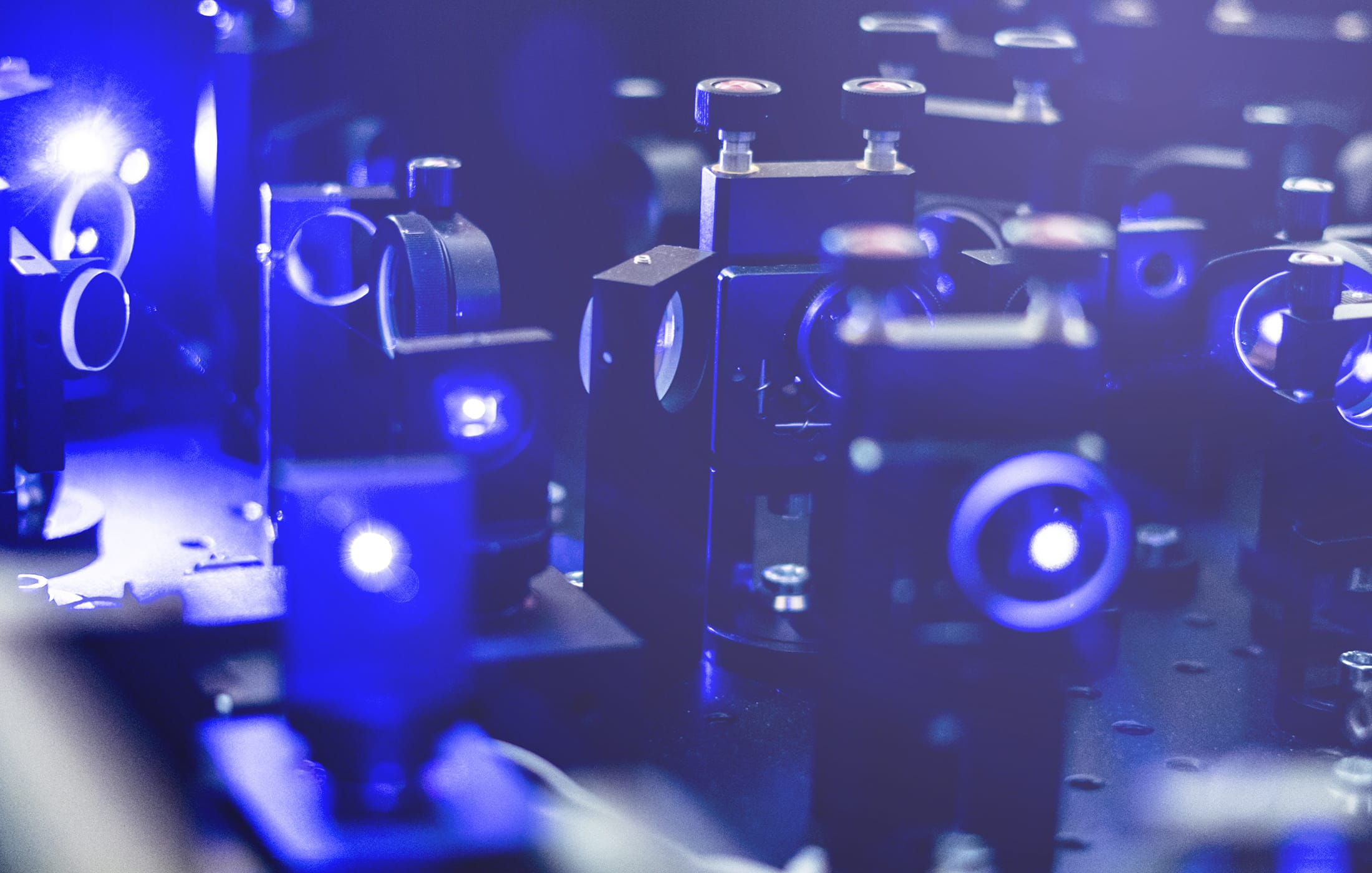
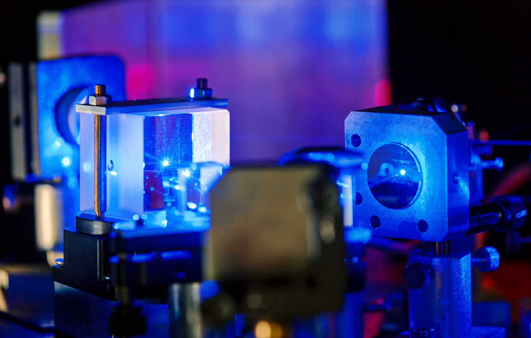
Photonic’s qubit modality is a hybrid of solid-state spins and photonics. The qubits are spin defects in silicon (specifically the T-centre defect) that have an optical transition at telecom wavelengths. Each qubit can thus interact with light – absorbing or emitting single photons that carry quantum information. These spins are hosted in silicon-28 (a spin-free silicon isotope), which offers long spin coherence times, and they can be controlled by both laser pulses and electrical signals (via on-chip p-i-n diode structures). Photonic integrates these qubits into silicon photonic chips: nano-fabricated waveguides, gratings, and cavities route photons between qubits and off-chip fiber interfaces. In essence, each module is a silicon photonic chip with multiple T-centre qubits and an optical circuitry backplane, plus electronic controls for initializing and manipulating the spins. Qubits on the same chip can be entangled through on-chip photonic circuits, and qubits on different chips (or in different cryostats) are entangled by sending photons through optical fiber between the chips. This yields a distributed quantum processor – a collection of smaller quantum nodes connected into one logical machine via optical entanglement.
Strengths – Silicon + Photons:
- CMOS Manufacturability: Because qubits are built in silicon, Photonic’s hardware can leverage the huge advances of the semiconductor industry. Silicon fabrication techniques (implantation, lithography, CMOS processing) can potentially produce qubit chips in large volumes with high precision. This is a stark contrast to, say, superconducting circuits that require specialized fabrication, or trapped ions that are assembled individually. If T-centre qubits can be reliably embedded across a wafer, one can imagine scaling to thousands or millions of qubits by tiling many silicon chips – a task well-suited to existing microelectronics factories. As researchers noted, “developing quantum technology using silicon provides opportunities to rapidly scale… since silicon photonics and electronics manufacturing is well-established”. Photonic’s approach could piggyback on this infrastructure, making quantum hardware more reproducible and ultimately cheaper to deploy.
- Native Telecom Networking: The choice of a telecom-wavelength optical interface (around 1310 nm O-band) is a major advantage. Photons at these wavelengths experience minimal loss in standard optical fibers, enabling long-distance quantum links between qubits. In Photonic’s design, every qubit is effectively “network-ready” – it can send entangled photons directly into fiber networks. This means modules can be physically separate (even in different data centers) and still form a single quantum computer, or conversely, multiple distant users could share entangled qubits for quantum communication. The platform inherently supports a quantum internet style scaling. By using telecom fiber, Photonic avoids the need for exotic quantum interconnects; it integrates with the same fiber tech that underpins the classical internet This modularity and range are key to horizontal scalability.
- High Connectivity for Error Correction: Within a Photonic module and across modules, qubits can be highly interconnected as a graph, thanks to the photonic links. Any two qubits that can exchange photons (directly or via intermediate nodes) can become entangled. This graph connectivity is far richer than a 2D grid (like in many superconducting qubit chips). The benefit is in quantum error correction: schemes like photonic cluster states or QLDPC codes thrive on connectivity. Photonic’s hardware can perform entangling operations between non-neighboring qubits with relative ease via optical interference, enabling low-overhead error correction codes that aren’t viable on sparse architectures. The company specifically touts that it can implement quantum LDPC codes requiring long-range links, thus achieving fault tolerance with far fewer qubits. In practical terms, this could mean a smaller, more scalable system to reach the same error-corrected computational power.
- Hybrid Control (Optical & Electrical): Photonic has demonstrated that its silicon qubits can be controlled both by light and by electrical pulses. Recently they showed the first electrically driven single-photon source in silicon, using a diode to excite a T-centre and emit a photon. They also electrically pulsed a single T-centre and achieved spin initialization via the emitted photons. The ability to use standard electronics (instead of multiple laser beams) to control qubits is a big win for scalability. Hundreds of qubits can be wired to electronic controllers (much like wiring transistors on a chip), which is far more scalable than aligning hundreds of lasers. Electrical control allows parallel operation on many qubits – e.g. triggering many qubits with synchronized voltage pulses – which is critical as qubit counts grow. Photonic’s design thus combines the fast, parallelizable control of classical electronics with the quantum connectivity of photonics.
- Long Memory & No Idle Decoherence (Potential): Solid-state spins in silicon (especially nuclear spins) can have very long coherence times – sometimes seconds or more – when isolated. If Photonic can utilize nuclear spin memory (e.g. the T-centre’s nuclear spin) for storage, qubits could effectively pause without losing state, which is helpful for networking and waiting for communication latency. Photons, meanwhile, travel at the speed of light and don’t decohere in transit (aside from loss), which means distributing entanglement doesn’t introduce significant additional decoherence. In contrast, many other qubit types (superconductors, ions) suffer decay if you simply wait or communicate over distance. Photonic’s architecture could store qubits as spins and communicate with photons, minimizing idle errors. (This strength will depend on engineering details – as of now the demonstrated T-centre electron spin coherence is promising but will need to be maintained with larger devices.)
Trade-offs and Challenges – “Networked” Quantum Computing:
- Complex Architecture: Photonic’s system is arguably more complex than a single-chip quantum processor. It combines cryogenic electronics, photonic circuitry, defect qubits, fiber interconnects, and synchronization of remote modules. Building each piece is challenging; integrating them seamlessly is even harder. For instance, fabricating chips with hundreds or thousands of T-centre qubits at specific locations, each coupled to a photonic cavity and a waveguide, pushes the limits of silicon defect engineering. Ensuring uniform qubit properties (frequency alignment, coherence, etc.) across a large chip or many chips is non-trivial. This complexity means there are more potential points of failure or yield issues compared to a simpler monolithic device.
- Cryogenic Operation: Despite using “telecom” photons, the T-centre spin qubits currently operate at cryogenic temperatures (the experiments are done at ~1.5–4 K range). This is warmer than superconducting qubits’ millikelvin regime, but still requires cryostats or dilution refrigerators for large systems. Managing many cryogenic modules and the fiber connections between them is an engineering challenge. Photonic will need to show that its modules can be reliably cooled and run 24/7, and that connecting fibers between cryostats doesn’t introduce too much thermal load or loss. The company does claim its approach can “operate under diverse environmental conditions” and integrate into standard data centers, but that remains to be proven at scale. Cryogenics adds complexity in cooling power and infrastructure as the system grows.
- Entanglement Rate and Latency: In distributed quantum computing, the speed of two-qubit operations is limited by how fast you can distribute entanglement between modules. Currently, optical entanglement between remote solid-state qubits is relatively slow (often kilohertz-scale). Photonic’s demo entangled two modules, but likely at modest rates. They have a target to achieve ~200 kHz entanglement with 99.8% fidelity in the future, which would be a huge improvement. Even 200 kHz, however, is slower than on-chip gate speeds for some other platforms (which can be MHz). This means algorithms spanning multiple modules might run with higher latency. Photonic can mitigate this by parallelizing entanglement attempts (many fiber channels, multiplexed photons) and by using error correction to tolerate some latency. Nonetheless, getting entanglement rates to the hundreds of kHz or more is a technical hurdle – it requires extremely efficient single-photon sources, low-loss optics, and fast detectors. Any inefficiency (photon loss, detector dead-time, etc.) reduces the entangling speed. As one expert noted, Photonic’s path to 200 kHz with 99.8% fidelity is “very striking” but also sets a high bar that others will be pressured to follow. Achieving that will require pushing photonics technology to its limits (e.g. high-Q cavities, superconducting nanowire detectors, etc.) Until then, the networked approach might have slower raw gate speeds, potentially offset by the ability to scale qubit numbers.
- Probabilistic Entanglement & Overhead: The optical entanglement between qubits (likely via interference of photons and heralding) is probabilistic – not every attempt succeeds in entangling the qubits. Photonic’s design must contend with this by re-trying failed entanglement attempts or having multiple attempts in parallel. This introduces some overhead and complexity in orchestrating operations. The good news is failed attempts are known (heralded by lack of a detector click), so they primarily cost time. But if too many operations in a computation rely on probabilistic entanglement, the runtime can become slow or variable. Photonic will aim to make entanglement success rates high (via better photon collection and coupling) to minimize this issue. There’s also a need for sophisticated scheduling and classical control to manage these distributed operations in real-time.
- Defect Qubit Challenges: Working with atomic-scale defects in silicon carries its own challenges. Each T-centre is essentially a tiny “quantum dot” inside the crystal. Variability in their local environment can cause inhomogeneities – e.g. slight frequency differences or spectral diffusion (frequency drift) of the photons. Photonic will need to implement techniques to tune and stabilize each qubit (perhaps via applied strain, electric fields, or dynamic feedback). Additionally, while silicon is a friendly host (minimal nuclear spins in isotopically purified Si-28), any residual impurities or fabrication damage could impact qubit coherence. Achieving high-fidelity gates between two spins on the same chip is another step that Photonic must demonstrate; likely they will use optical two-qubit gates which must be precise. Until now, much of the work has been about linking and initializing qubits; full logic operations among many silicon spin qubits (with error rates low enough for QEC) are still on the to-do list.
- Competition and Technological Risk: Photonic’s approach is innovative but relatively unproven compared to, say, superconducting qubits or trapped ions which have demonstrated 50–100 qubit devices running small algorithms. There is a risk that some unforeseen obstacle (materials issues, noise sources, etc.) could slow down progress. Also, other companies are racing toward fault-tolerance (IBM plans ~100,000 qubits by 2033, IonQ and Quantinuum are pursuing photonic interconnects too, PsiQuantum is pursuing a purely photonic route, etc.). Photonic will need to maintain a steep progress curve to stay ahead. Their bold claims raise expectations – any significant delay or unmet milestone could invite skepticism. Essentially, executing perfect integration of quantum computing and networking is a multi-front challenge, and Photonic must advance on all fronts (qubit quality, optical connectivity, error correction software, scaling engineering) simultaneously. This is high-risk, high-reward territory.
In summary, Photonic’s silicon photonic modality offers tantalizing scalability and connectivity advantages, but it comes with the complexity of uniting two frontier technologies (quantum computing and quantum networking). The strengths – manufacturability, telecom networking, and inherent modularity – make it one of the more scalable architectures on paper. The trade-offs lie in the practical difficulties of implementation and ensuring that a distributed system can operate as fast and accurately as a monolithic one. Over the next few years, we can expect Photonic to address these challenges one by one. If they succeed, the payoff is huge: a path to essentially unlimited scaling of qubits by adding more networked modules, fulfilling the promise of an “infinitely scalable” quantum computer built like an internet of quantum nodes.
Track Record
Although Photonic Inc. is a young company, its track record to date shows a pattern of setting bold goals and meeting them (or even exceeding them) on an aggressive timeline.
Since its founding, Photonic has hit several technical and strategic milestones when it said it would, instilling confidence in investors and partners. For example, in 2023 Photonic proclaimed it would demonstrate key features of its distributed architecture within a year – and indeed by mid-2024 it had experimentally verified distributed entanglement and remote quantum gates between silicon qubits. The company also asserted that efficient error correction was on its near-term roadmap – and in early 2025 it delivered a breakthrough in the form of SHYPS QLDPC codes, along with a scientific paper and simulations to back it up. These achievements suggest Photonic’s team has been executing swiftly and on schedule. It’s worth noting that Dr. Simmons and colleagues had been steadily advancing the underlying science for years prior – progressing from single T-centre qubit experiments in 2020, to photonic chip integration in 2022, to electrical control in 2025. Each step was published in high-impact journals (e.g. Nature in 2022 for the photonic integration, Physical Review X Quantum in 2023 for the architecture, etc.), highlighting that Photonic’s claims are grounded in peer-reviewed research. This close partnership between academia and the startup has accelerated the translation of lab results into prototype devices.
On the corporate side, Photonic’s track record is marked by rapidly gained credibility. Their fundraising success and partnerships speak volumes: securing $140 M with participation from a tech giant (Microsoft) and top-tier investors by 2023 indicates that Photonic hit the technical milestones set in earlier funding rounds. According to BCI’s CIO, Photonic had “reached several major technical milestones” and established key partnerships between their initial investment and the big 2023 round. In other words, the company delivered enough progress to justify increasing bets from stakeholders. Photonic also won competitive grants/endorsements, such as being a semifinalist in Canada’s national quantum technology challenges and the DARPA QBI selection. Each of these vetting processes (with extensive due diligence by experts) further validates Photonic’s track record and approach.
Another aspect of Photonic’s execution is its ability to attract top talent and advisors. By assembling one of the largest teams of quantum silicon experts (150+ staff including veterans from quantum labs and industry), Photonic ensured it has the human capital to meet its roadmap. They’ve also expanded operations internationally (opening offices and labs in the US and UK) to tap global expertise and resources. This rapid scaling of the team and footprint, while maintaining a clear technical focus, is often a sign of a well-managed deep-tech startup. Moreover, Photonic’s leadership is active in the quantum community (Dr. Simmons co-chairs Canada’s National Quantum Strategy advisory board, the CEO and others speak at major conferences). This suggests they are keeping a pulse on and contributing to the broader ecosystem, which can only help in staying on track and forming the right collaborations.
So far, Photonic has not publicly missed any announced milestones – if anything, they sometimes kept developments under wraps until achieving them (e.g. the QLDPC code breakthrough was a surprise to many in the field). Of course, the hardest parts of the journey are still ahead: scaling from demos to a full prototype will test the company’s mettle. But if past performance is any indicator, Photonic will continue to iterate quickly and hit interim goals. Industry analysts have taken note: Global Quantum Intelligence’s David Shaw remarked that Photonic’s recent demos “set a new bar for quantum roadmaps that others will be under pressure to follow… [this] stands to accelerate the industry“.
In other words, Photonic is building a reputation for leading on timeline and delivery, not lagging. It is carving out a niche as the startup that may leapfrog more established players by doing the hard things (networking, QEC) early. Time will tell if they can keep up the pace, but as of 2025 their track record inspires cautious optimism that they might just achieve their daring goal of a useful quantum computer on an accelerated schedule.
Challenges
Despite its strong momentum, Photonic Inc. faces formidable challenges on the road to a commercial quantum computer. Some of the key challenges and risks include:
- Scaling Up Qubit Production: Thus far, experiments have involved at most a handful of T-centre qubits. To build a useful machine, Photonic will need to create chips containing perhaps thousands of T-centre qubits, all reliably functioning. Implanting or fabricating that many identical defect qubits in silicon with high yield is uncharted territory. Each qubit must couple to control electrodes and photonic structures; any variability could affect performance. This is a manufacturing and materials challenge: developing techniques to produce and tune large arrays of spin-photon qubits. Photonic’s use of silicon and CMOS fab methods gives it a fighting chance, but until a prototype with, say, 50-100 qubits is demonstrated, scalability remains a big question mark.
- Maintaining Qubit Quality at Scale: Even if qubits can be made in quantity, their coherence and fidelity must remain high as the system grows. More qubits and components mean more sources of error (e.g. optical loss, crosstalk, spectral diffusion). The T-centre qubit’s performance in small demos has been good, but will those metrics hold in a densely integrated device? Error rates need to be extremely low for error correction to work (e.g. gate fidelities 99.9%+). Each additional component (beam splitter, fiber connector, etc.) could introduce loss or noise. Photonic has to engineer around these issues – improving photon collection efficiency, stabilizing qubit frequencies, and possibly using techniques like active feedback or dynamic error suppression. In essence, scaling must not come at the cost of qubit quality; balancing quantity and quality is a central challenge.
- System Integration and Engineering: Photonic’s end goal looks more like a quantum data center than a simple box. They will have multiple cryogenic modules, each with perhaps dozens of qubits, all linked by fibers, with precise timing and classical orchestration. Integrating this into a functional system is non-trivial. Issues like thermal management (many cryostats and fiber feeds), vibrational stability (to maintain alignment of optics), and timing synchronization (photons arriving within femtoseconds for interference) need to be solved. The classical control architecture that manages qubit operations across the network must be extremely fast and coordinated, likely distributing clock signals and feed-forward information among nodes. Essentially, Photonic has to build a distributed computing system where the “processors” are quantum modules and the interconnect is optical. This is a new paradigm that will require innovative engineering in hardware and software. Any hiccup in synchronization or communication could decohere the fragile quantum states.
- Achieving Fault-Tolerance Thresholds: While Photonic’s QLDPC codes promise lower overhead, they still require an error rate below a certain threshold to start netting improvements. The company must bring physical error rates into the regime where error-corrected logical qubits are stable and beneficial. This likely means two-qubit gate error rates on the order of 1e-3 or better, photon loss per link well under a percent, and sufficiently fast cycle times. If physical error rates are too high, even the best codes won’t yield a stable logical qubit. Photonic will need to iterate on qubit design and error mitigation (dynamic decoupling for spins, better cavity coupling for photons, etc.) to reach those thresholds. Additionally, implementing the QLDPC code in hardware control systems is a heavy lift – it requires fast decoding algorithms, many parallel operations, and handling the more complex syndrome measurements of LDPC codes. In short, turning the promise of SHYPS codes into reality will be a major challenge; it’s one thing to publish a paper, another to get it running on real hardware with all error sources in play.
- Timeline and Execution Risk: Photonic’s public timeline (“5 years to a fault-tolerant solution”) is extremely ambitious. Hitting that would require nearly flawless execution and maybe a bit of luck in discovery. Any number of setbacks – a material issue, a delay in a critical component, difficulty in hiring specialized talent – could push out the schedule. The quantum industry is littered with overly optimistic projections that didn’t pan out on time. Photonic must manage expectations and avoid over-promising to maintain credibility. So far, they’ve delivered on early milestones, but the complexity grows exponentially from here. There is a risk of a “hardware valley of death”, where translating principles into a full system reveals unforeseen problems (like how to route thousands of fibers, or how to calibrate 1,000 qubits). The company’s ability to project manage large-scale R&D will be tested. They will likely need to expand partnerships (with industrial fabs, optical manufacturers, etc.) to get all the pieces in place in time. Missing a self-imposed deadline wouldn’t be unusual in this field, but since Photonic has touted a faster timeline than others, any significant delay might affect how they are perceived by investors or customers.
- Competition and First-to-Market Pressure: While Photonic works on its approach, competitors are not standing still. Tech giants like IBM, Google, and Intel are pursuing their own scalable quantum roadmaps (superconducting and spin qubits), startups like PsiQuantum and Xanadu are pushing photonic approaches, and ion trap systems are also improving. It’s possible that a competitor achieves a major breakthrough (e.g. a thousand-qubit error-corrected system) before Photonic does, which could narrow Photonic’s window to lead. There’s also convergence in ideas: for instance, IonQ and Quantinuum plan to network ion-trap modules with photons (conceptually similar to Photonic’s distributed approach), and Microsoft is developing its own spin-photon qubits (though with topological qubits in mind). Photonic will have to maintain a technological edge and demonstrate tangible advantages (like significantly lower qubit overhead or easier scaling) to stay ahead. This competitive pressure is a challenge in itself – it can be a motivator but also adds urgency that can stress a team.
- Regulatory/Security Considerations: On a different note, as Photonic’s technology matures, it may attract government regulation or security scrutiny, given its dual-use nature (powering breakthroughs but also breaking cryptography). The company is already involved with defense agencies (DARPA, Canadian DND), which means aspects of their work might become classified or subject to export controls. Navigating collaboration with governments while also trying to commercialize broadly can be challenging. They will need to manage IP carefully (DARPA’s QBI allows companies to keep IP, but still, anything touching defense can complicate open commercialization). If their system becomes a frontrunner for CRQC, governments might impose restrictions or require certain safeguards. This is a “good problem” in that it means the tech is succeeding, but it’s a non-technical challenge that could influence Photonic’s trajectory and market deployment.
In light of these challenges, Photonic’s journey is far from guaranteed to be smooth. The company has significant toil ahead to turn its prototypes into a full-fledged quantum computer. As I previously noted, “there are many engineering challenges remaining… we’re not at a cryptographically relevant quantum computer yet, and this achievement doesn’t suddenly enable code-breaking – it demonstrates a new capability that could make future processors easier to scale”. This nicely captures Photonic’s situation: each advance is a stepping stone, but many more steps must follow. The upside is that Photonic has identified the major hurdles and is tackling them head-on (scalability, connectivity, error correction). By confronting the hardest problems early, they give themselves more time to iterate solutions. If they continue to gather talent and support, and keep hitting intermediate goals, Photonic could very well overcome these challenges.
Quantum Upside & Quantum Risk - Handled
My company - Applied Quantum - helps governments, enterprises, and investors prepare for both the upside and the risk of quantum technologies. We deliver concise board and investor briefings; demystify quantum computing, sensing, and communications; craft national and corporate strategies to capture advantage; and turn plans into delivery. We help you mitigate the quantum risk by executing crypto‑inventory, crypto‑agility implementation, PQC migration, and broader defenses against the quantum threat. We run vendor due diligence, proof‑of‑value pilots, standards and policy alignment, workforce training, and procurement support, then oversee implementation across your organization. Contact me if you want help.
Related Content