Electrically Triggered Spin-Photon Device Demonstrated in Silicon
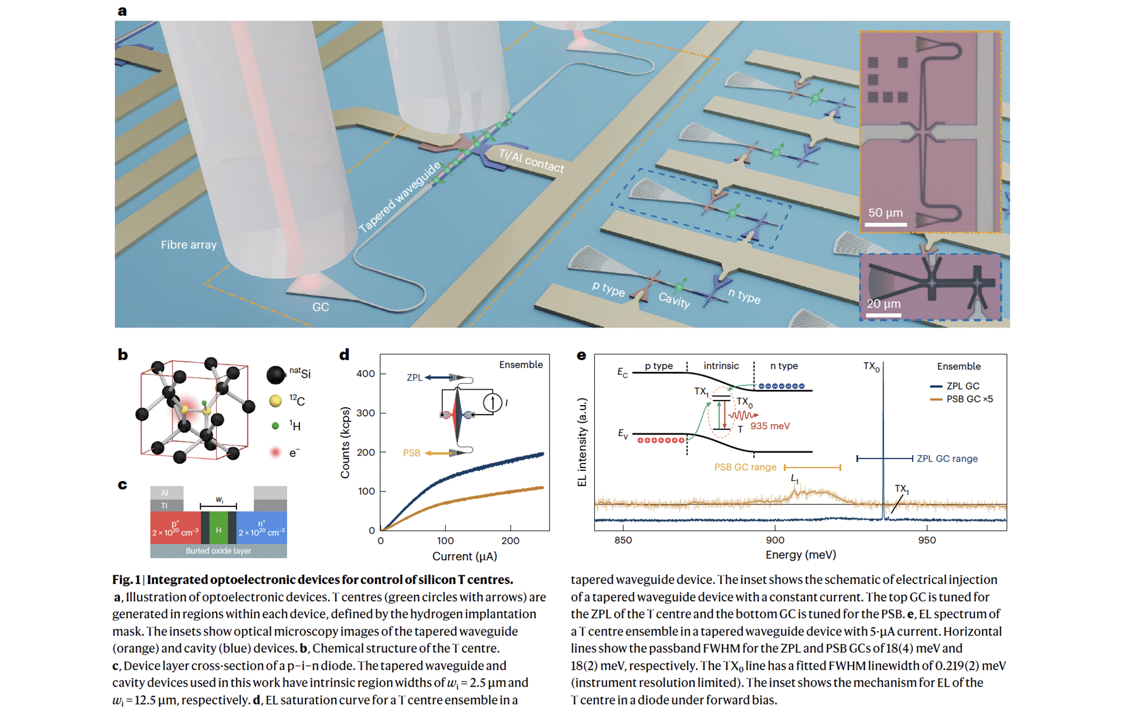
Table of Contents
13 Sep 2025 – A new research paper titled “Electrically triggered spin-photon devices in silicon” has been published in Nature Photonics on September 11, 2025. In this paper, a team from Simon Fraser University (SFU) and quantum startup Photonic Inc. report the first of its kind electrically injected single-photon source built on a silicon chip.
This breakthrough marks an important step toward scalable quantum computing hardware, as it shows that silicon-based qubit devices can be controlled not only with laser light but also with standard electrical signals. The achievement addresses a key challenge in quantum tech by integrating quantum light sources and spin qubits into mainstream semiconductor technology.
What Did the Researchers Achieve?
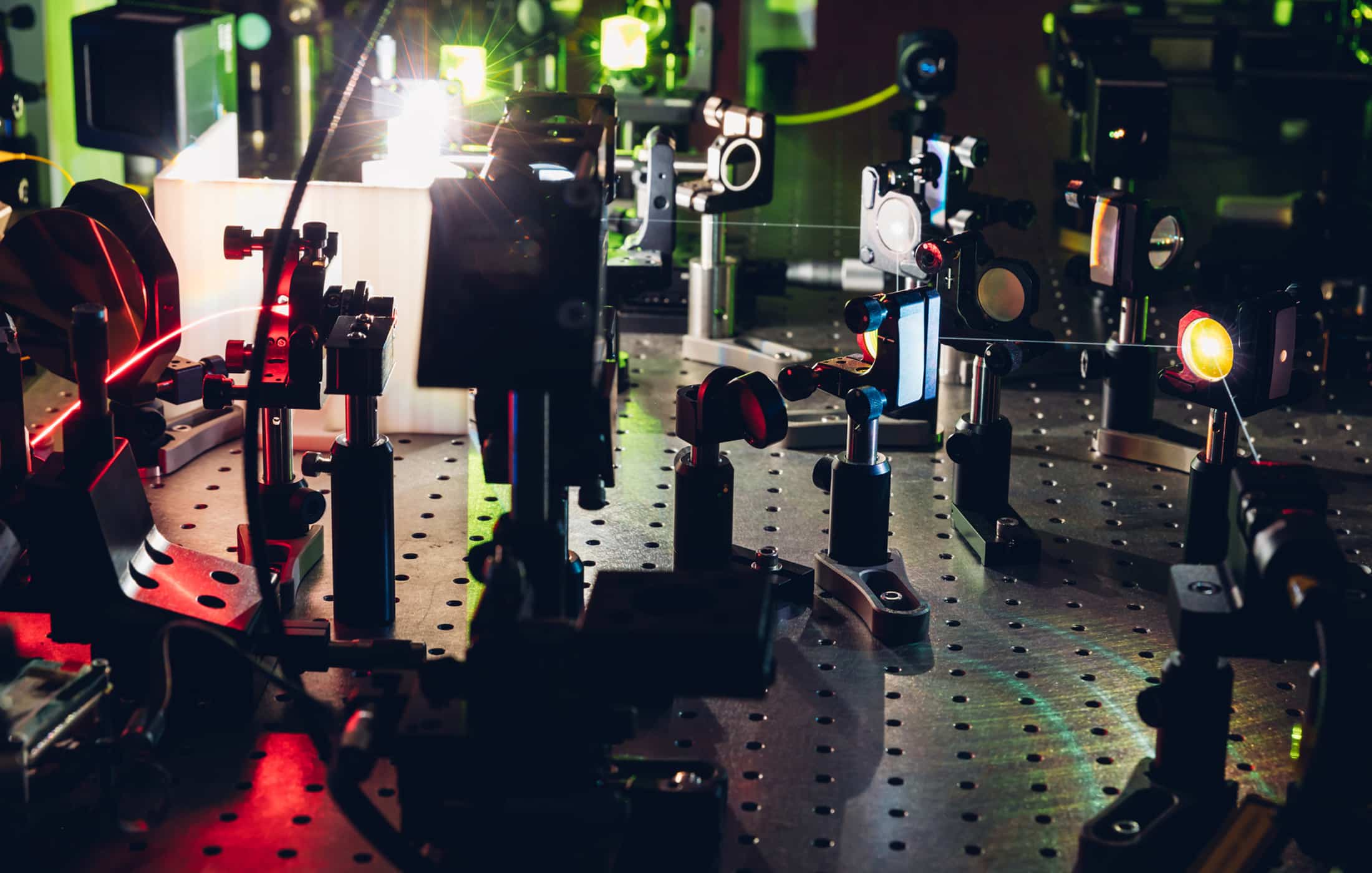
In this study, the researchers developed two types of on-chip devices that harness optically active spin defects in silicon called T-centres. T-centre defects (two carbon atoms and one hydrogen substituting into silicon) are known to emit photons at telecom wavelengths (~1326 nm) and can serve as quantum bits (spins). By fabricating nanophotonic circuits on a silicon wafer and implanting T-centres inside p-i-n diode structures, the team created the following devices :
- Silicon LED (O-band light source): First, they demonstrated an on-chip light-emitting diode where an electrical current excites an ensemble of T-centres. This device emitted light in the telecom O-band (~1.3 µm), showing that silicon T-centres can be driven electrically to produce light. This is essentially a nanoscale LED in silicon that works at cryogenic temperatures, and it could be useful as a compact light source for cryogenic classical or quantum optical systems.
- Single-Photon Emitter: Next, they built a nanocavity around a single T-centre to create an electrically triggered single-photon source. When a voltage pulse is applied to the diode, a single T-centre is excited and emits single photons into the silicon waveguide. The emission was coupled into an integrated cavity to enhance its intensity. This is the first time anyone has electrically driven a silicon defect to generate single photons, a major milestone for on-chip quantum light sources.
- Heralded Spin Initialization: Importantly, the team also demonstrated a new method to initialize the spin state of the T-centre qubit using its emitted photon. In practice, they sent a series of electrical excitation pulses to the T-centre and used a spectral filter and single-photon detector to catch photons of a specific wavelength. Detection of a photon from a particular optical transition heralds that the T-centre’s electron spin collapsed into a certain state. By post-selecting on those heralding events, they prepared the electron spin in a known state with ~92% fidelity. This “heralded spin initialization” is a clever way to set or reset qubits via emitted photons, without needing separate laser-based spin pumping for each qubit. It’s a new technique enabled by the electrically driven optical transitions of the T-centre.
In summary, the researchers showed that a silicon chip can integrate quantum defects that are controlled both by light and by electrical pulses. The devices function as electrically activated sources of single telecom-band photons and as a means to read/write the quantum spin state of the defects. All of this was achieved using silicon nanofabrication techniques compatible with conventional CMOS photonics, highlighting the marriage of quantum physics with existing chip technology.
Why Is This Important?
This achievement is exciting for several reasons:
First Electrical Quantum Light Source in Silicon: Until now, optically active qubits in solids (like color centers in diamond or silicon) were typically excited with lasers. Here we have the first electrically injected single-photon source in silicon. In the words of the authors, “Previously, we controlled these qubits… optically. Now we’re introducing electrical control as well, which increases the device capability and is a step toward applications in a scalable quantum computer.” Electrical control means we can trigger quantum light emission using standard electronic pulses (just like driving a semiconductor LED), which is much more scalable for integrating large numbers of qubits. No individual alignment of laser beams is needed for each emitter.
Silicon-Based Qubits & CMOS Compatibility: The work uses silicon as the host platform – the cornerstone of modern electronics. The global semiconductor industry can already mass-produce silicon chips with extraordinary precision and low cost. By demonstrating quantum devices in silicon, this research paves the way to leverage existing fabrication infrastructure for building quantum hardware. It’s far easier to imagine scaling up to thousands or millions of qubit devices if they can be made using silicon wafer processes, as opposed to exotic materials. “Developing quantum technology using silicon provides opportunities to rapidly scale quantum computing,” the team noted, since silicon photonics and electronics manufacturing is a well-established backbone of the tech industry.
Telecom-Band Operation for Networking: The T-centre emits photons in the telecommunications bands (the O-band around 1326 nm). This is a big deal because telecom wavelengths are the ones that travel with minimal loss in optical fibers. Quantum communication and quantum internet applications demand sources of indistinguishable single photons at telecom wavelengths to send quantum information over long distances. The authors point out that such single-photon sources compatible with silicon photonics are a valuable resource for quantum communication networks and all-optical quantum computing architectures. The devices they built are already fiber-coupled on the chip, meaning they can directly interface with fiber networks or other on-chip photonic components. This could enable distributed quantum networks connecting multiple silicon chips.
Parallel Qubit Control and Scaling: By introducing an electrical method to excite and initialize spins, this work offers a path to highly parallel control of many qubits. The paper notes that future quantum processors may require hundreds of thousands of qubits for commercial applications, which makes per-qubit optical control cumbersome. Using on-chip electrical pulses and on-chip photonic filters/detectors, many T-centre qubits could potentially be initialized or entangled simultaneously rather than one-by-one with separate lasers. This parallelism is crucial for scaling up. In their discussion, the authors compare their method to having huge optical switching networks (which would be needed to direct laser light to each qubit) – an electrical approach can simplify that by leveraging integrated circuits to drive many qubits at once. In short, it’s a more system-level efficient approach to controlling a large quantum chip.
Towards Practical Quantum Processors: The SFU/Photonic Inc. team has been steadily advancing silicon T-centre technology for a few years. In 2020 they first identified single T-centres as quantum bits, in 2022 they integrated them into photonic structures, and now in 2025 they’ve added electrical injection and control. Each step unlocks more capabilities you need to build a useful computer. The close collaboration with industry (Photonic Inc.) also signals that these advances are being translated toward commercial quantum devices. Photonic Inc. provided advanced nanofabrication to make the diode nanocavity chips and is aiming to build commercial-scale quantum computers and networks based on this tech. This kind of academic-industry partnership accelerates the path from lab result to real-world systems.
Does This Bring Q-Day Any Closer?
Q-Day is a term often used to denote the day when a quantum computer becomes powerful enough to break contemporary cryptographic protocols (for example, cracking RSA-2048 encryption). It’s essentially the “quantum apocalypse” moment for classical encryption, after which all sensitive communications could be at risk if not protected by quantum-safe (post-quantum) cryptography. So, does this silicon T-centre breakthrough accelerate the arrival of Q-Day?
The short answer is not immediately, but it’s part of a larger trend bringing Q-Day closer bit by bit. This research is a hardware milestone that clears another hurdle toward building a scalable quantum computer. It shows a new way to integrate qubits and photonic links on a chip, which is exactly the kind of innovation needed to eventually scale up to the huge number of qubits required for breaking encryption.
However, the device demonstrated is still a single (or few) qubit system in a controlled laboratory setting. To threaten RSA or other encryption, a quantum computer would likely need millions of physical qubits or on the order of hundreds of thousands of error-corrected logical qubits working in concert. Tech industry roadmaps suggest that on the order of 100,000+ qubits might be needed to run Shor’s algorithm on RSA-2048 in a reasonable time. For instance, IBM has openly aimed to build a ~100,000-qubit quantum machine by the early 2030s – a scale believed sufficient to break RSA-2048.
The silicon T-centre platform is promising for reaching large qubit counts in the long term because it’s compatible with manufacturing scale-up. But there are many engineering challenges remaining: these devices currently operate at cryogenic temperatures, the per-qubit error rates and coherence times will need to be optimized, error correction schemes have to be implemented, and so on. In other words, we’re not at a cryptographically relevant quantum computer yet, and this particular achievement doesn’t suddenly enable code-breaking algorithms. What it does do is demonstrate a new capability that could make future quantum processors more practical and easier to scale – which in turn contributes to the overall progress of quantum computing.
Quantum Upside & Quantum Risk - Handled
My company - Applied Quantum - helps governments, enterprises, and investors prepare for both the upside and the risk of quantum technologies. We deliver concise board and investor briefings; demystify quantum computing, sensing, and communications; craft national and corporate strategies to capture advantage; and turn plans into delivery. We help you mitigate the quantum risk by executing crypto‑inventory, crypto‑agility implementation, PQC migration, and broader defenses against the quantum threat. We run vendor due diligence, proof‑of‑value pilots, standards and policy alignment, workforce training, and procurement support, then oversee implementation across your organization. Contact me if you want help.
Related Content