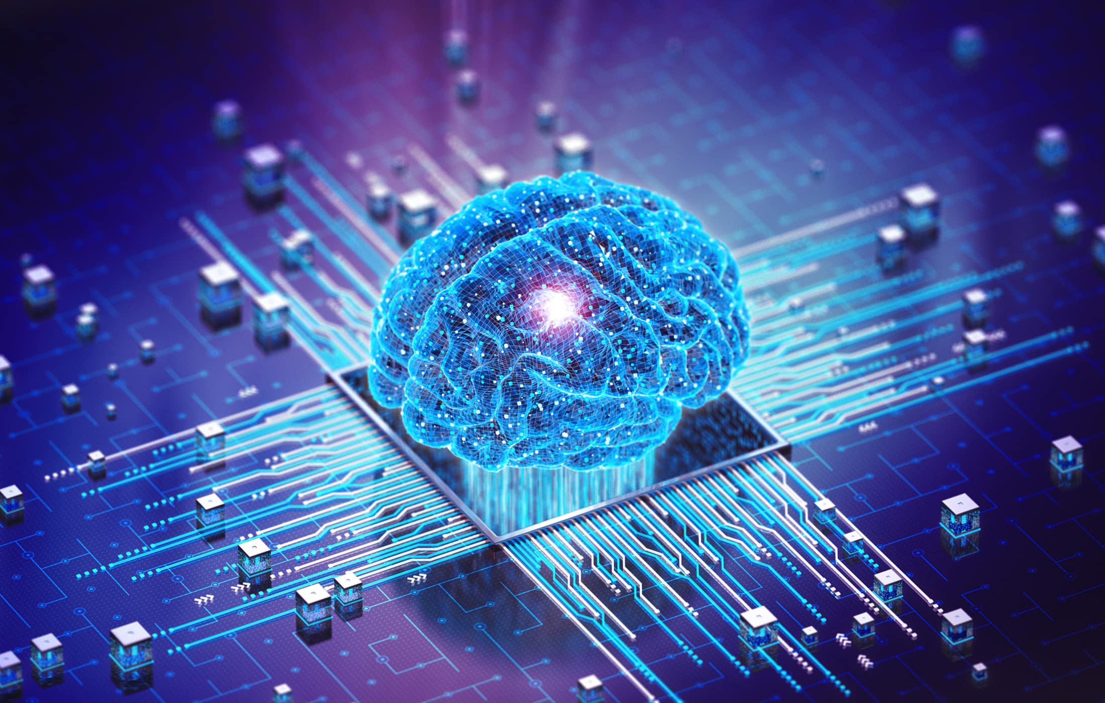
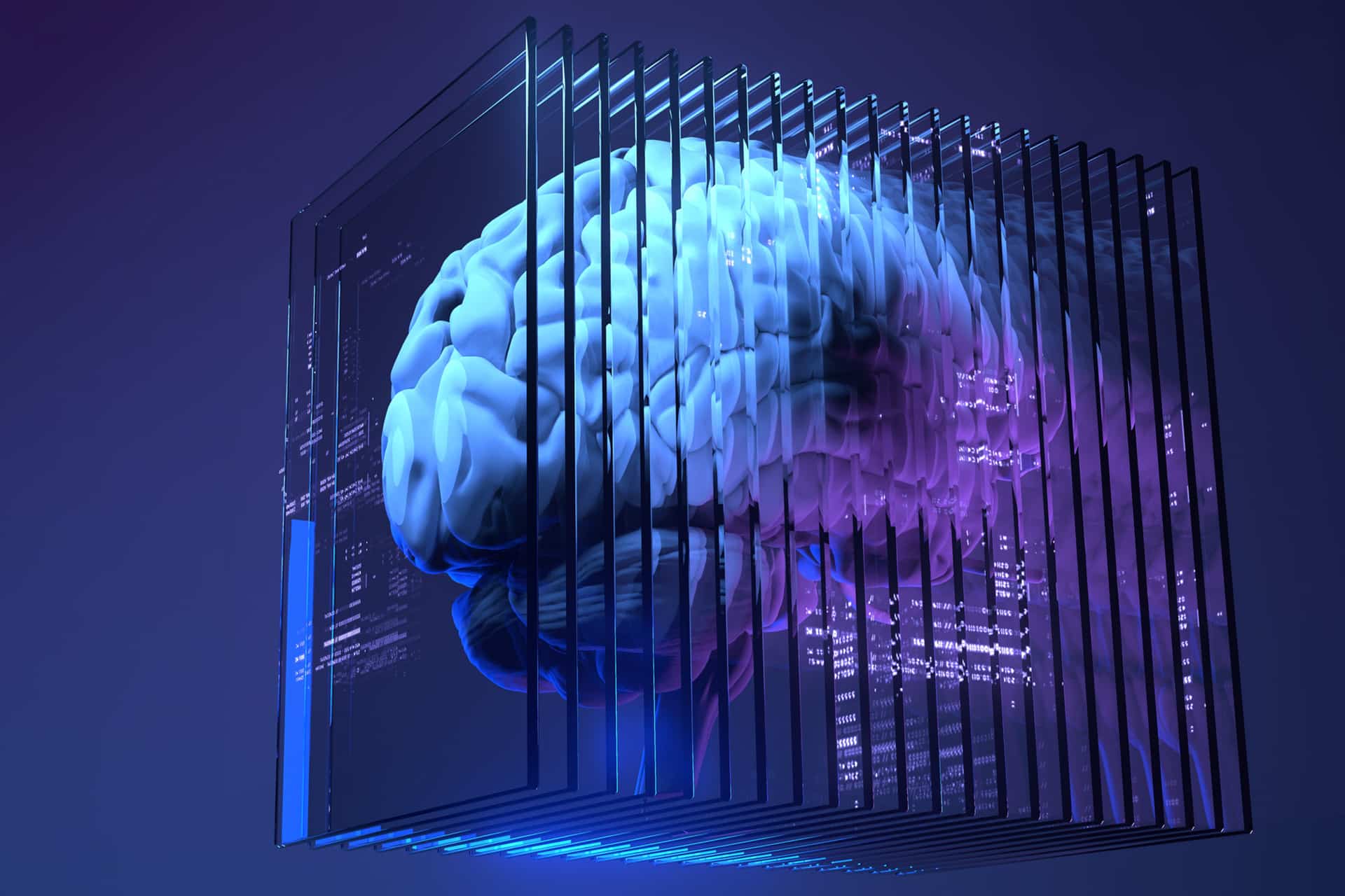
China’s “Photonic Quantum Chip” Is Impressive. But It’s Also a Case Study in Quantum-Washing
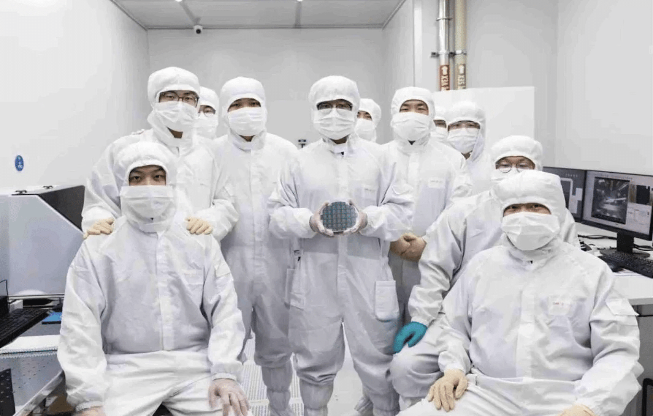
Table of Contents
Every few months, a headline pops up proclaiming the dawn of a new quantum breakthrough – often accompanied by phrases like “1000x faster than classical computers,” “industry first,” “quantum chip,” or “beyond classical limits.” And every time, the quantum-security community winces. Not because these technologies aren’t exciting, they often are, but because the language steadily erodes public understanding of what quantum computing actually is, and what it isn’t.
The latest example arrived from China, where the Chip Hub for Integrated Photonics Xplore (CHIPX), working with start-up Turing Quantum, unveiled what the media quickly dubbed a “photonic quantum chip”. It won the “Leading Technology Award” at the 2025 World Internet Conference in Wuzhen, and several outlets reported that it offers “1,000x acceleration”, “exceeds classical limits”, and is already deployed in aerospace, biomedicine, and finance.
It sounds like a genuine quantum leap.
Except it isn’t a quantum computer.
It’s something different and still interesting, but decidedly not what most headlines imply.
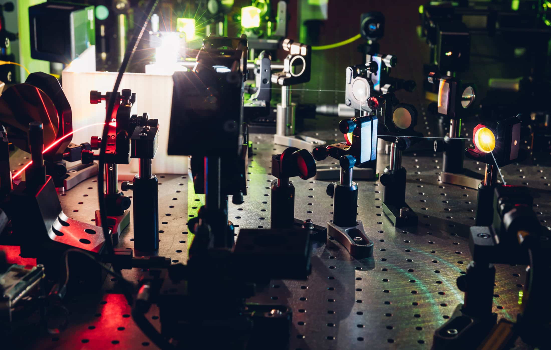
The Reality Behind the Hype: A Classical Photonic Processor
The most authoritative technical description of the hardware comes from the same CHIPX–Turing Q team, in a recent paper titled “A fully-programmable integrated photonic processor for both domain-specific and general-purpose computing”. It describes a programmable optical processor built using:
- Integrated Mach–Zehnder interferometer (MZI) meshes
- Phase shifters
- PIN photodiodes
- Continuous-wave classical lasers
- Thin-film lithium niobate (LiNbO₃) photonics
Nothing in the architecture uses single-photon sources, entanglement, cluster states, quantum gates, or any of the features that make a device meaningfully quantum.
Instead, the chip performs classical optical computing – fast, parallel, energy-efficient, and implemented entirely with bright light. The team demonstrates:
- Optical solvers for NP-complete problem instances
- MNIST digit classification
- Image convolution
- Linear algebra acceleration for ML workloads
This is accomplished by exploiting the natural parallelism of light interference in an MZI mesh, not by harnessing quantum superposition or entanglement.
In other words: it’s a photonic AI and optimization accelerator, not a quantum device.
So Why Call It a “Quantum Chip”?
Some of the misunderstanding stems from translation and branding. In Chinese, terms like 光子, 量子, and 光量子 are often used interchangeably in mainstream science coverage, creating a linguistic blur between “photonic chip,” “quantum chip,” and “optical-quantum chip.”
But there are deeper reasons:
- Photonic hardware is a long-term pathway toward quantum photonics. The same MZI meshes used here also appear in photonic quantum architectures (boson sampling, Gaussian cluster states, modular interferometers). The boundary between classical and quantum photonics is porous—but this chip sits squarely on the classical side.
- Turing Quantum markets itself as a quantum company. When your start-up name includes “Quantum,” every product tends to inherit that branding.
- China is signalling technological leadership. Label something “quantum,” and it gets attention from policymakers, investors, and media both domestically and internationally.
- We’re in a quantum hype cycle. With quantum company stocks surging and the global spotlight on “quantum advantage,” you can see the incentive structure at work.
None of this invalidates the underlying engineering. But it does create a communication problem – one that ultimately harms the field.
What the Chip Is (and Why It Still Matters)
Once you strip away the quantum gloss, there is still a genuinely impressive achievement here.
1. Co-packaged photonics + electronics
The team claims to have achieved chip-level co-packaging of photonics and electronics, with wafer-scale mass manufacturing, reportedly a first for this class of device. That’s strategically important. It mirrors the global trend toward co-packaged optics (CPO) for datacenters and HPC systems, where electrical I/O is becoming a bottleneck.
If China now has a scalable 6-inch thin-film LiNbO₃ pilot line, as reported, they have positioned themselves well in the global photonics manufacturing race.
2. A reconfigurable MZI mesh for general-purpose optical compute
This isn’t a one-off demonstrator. It appears to be a programmable optical compute unit capable of switching between:
- ML inference
- Signal processing
- Optimization solvers
- Combinatorial problem instances
Programmability has always been a major barrier to photonic accelerators. If CHIPX has solved that in a manufacturable way, that’s a meaningful step forward.
3. Hybrid photonic-electronic AI acceleration
Optical matrix multiplication is orders of magnitude more energy-efficient than electronic equivalents – a huge advantage for AI datacenters, especially as large models balloon into multi-trillion-parameter scales. This chip seems purpose-built for that future.
4. A legitimate industrial foundation for future photonic quantum computing
If China can produce sophisticated integrated photonic chips at scale today, they will be better positioned to build:
- Photonic qubit generators
- MZI-based quantum circuits
- Gaussian boson sampling machines
- Continuous-variable cluster state processors
So while this is not a quantum computer, it may help China build the supply chain and engineering expertise required for one later.
The 1,000× Speedup: Impressive or Illusion?
Many articles breathlessly report “1000-fold acceleration.” But the original research does not present:
- Controlled benchmarks
- Comparison against modern GPUs (H100, B200, TPUv5)
- End-to-end AI workload measurements
- Full-scale optimization benchmarks
Instead, the speedup seems to refer to estimated energy-per-operation, latency for specific small optical circuits, or comparisons against CPU-based baselines. That is interesting, but hardly evidence of general-purpose superiority.
And the claim that this chip “exceeds the limits of classical computers” is simply incorrect. The processor can be fully simulated classically because it uses classical light. It may be faster or more efficient, but it doesn’t cross into the regime of quantum computational advantage.
This is precisely the kind of claim that makes quantum-washing so damaging. It erodes trust not only in media coverage, but in the genuine achievements of researchers.
Why Quantum-Washing Matters
Quantum-washing isn’t just a harmless exaggeration. It distorts public expectations, misleads investors, and complicates global conversations about:
- Quantum readiness
- Q-Day timelines
- PQC deployment urgency
- National-level quantum investment strategies
If every photonic accelerator, cold-atom sensor, neural-network chip, or laser-interferometer gets labelled “quantum,” people will lose the ability to distinguish incremental progress from genuinely transformative breakthroughs.
And for those of us working in quantum security, this matters deeply. Misinterpreting device capabilities can:
- Overinflate fears of early Q-Day
- Or worse, create false reassurance that “quantum chips are already here, so quantum computing must be solved”
Quantum-washing undermines rational decision-making in both directions.
A Better Path Forward: Celebrate the Engineering, Not the Hype
CHIPX and Turing Quantum built something legitimately interesting:
- A reconfigurable optical processor
- Integrated with custom electronics
- Manufactured on thin-film LiNbO₃ at wafer-scale
- With clear applications in AI, HPC, and optimization
- And genuine relevance to future photonic quantum hardware
That’s worth celebrating on its own merits.
But calling it a “photonic quantum chip” does a disservice to the field, to the public, and even to the team’s own work. The device is strong enough to stand on its own – no quantum gloss needed.
As the quantum industry enters a volatile but exciting period, with rising expectations and surging valuations, we need clearer communication, not more ambiguity.
And that means calling out quantum-washing when we see it – while still giving credit where it’s due.
Quantum Upside & Quantum Risk - Handled
My company - Applied Quantum - helps governments, enterprises, and investors prepare for both the upside and the risk of quantum technologies. We deliver concise board and investor briefings; demystify quantum computing, sensing, and communications; craft national and corporate strategies to capture advantage; and turn plans into delivery. We help you mitigate the quantum risk by executing crypto‑inventory, crypto‑agility implementation, PQC migration, and broader defenses against the quantum threat. We run vendor due diligence, proof‑of‑value pilots, standards and policy alignment, workforce training, and procurement support, then oversee implementation across your organization. Contact me if you want help.
Related Content